A Physical Derivation of Wave Digital Elements
This section provides a ``physical'' derivation of Wave Digital Filters (WDF), which contrasts somewhat with the more formal derivation common in the literature. The derivation is presented as a numbered series of steps (some with rather long discussions):
- To each element, such as a capacitor or inductor, attach a
length of waveguide (electrical transmission line) having wave
impedance
 , and make it infinitesimally long. (Take the limit as
its length goes to zero.) A schematic depiction of this is shown in
Fig.F.1a. For consistency, all signals are Laplace transforms of
their respective time-domain signals. The length must approach zero
in order not to introduce propagation delays into the signal path.
, and make it infinitesimally long. (Take the limit as
its length goes to zero.) A schematic depiction of this is shown in
Fig.F.1a. For consistency, all signals are Laplace transforms of
their respective time-domain signals. The length must approach zero
in order not to introduce propagation delays into the signal path.
Figure F.1: a) Physical schematic for the derivation of a wave digital model of driving-point impedance  . The inserted
waveguide impedance is real and positive, but otherwise
arbitrary. b) Expanded view of the interior of the infinitesimal
waveguide section, also representing the termination impedance
as an impedance-step within the waveguide.
. The inserted
waveguide impedance is real and positive, but otherwise
arbitrary. b) Expanded view of the interior of the infinitesimal
waveguide section, also representing the termination impedance
as an impedance-step within the waveguide.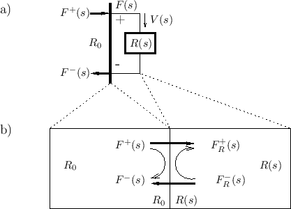
Points to note:
- The infinitesimal waveguide is terminated by the element.
The element reflects waves as if it were a new waveguide section at
impedance , as depicted in Fig.F.1b.
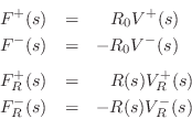
- The interface to the element is recast as traveling-wave
components
 and
and  at impedance .
In terms of these components, the physical force on the element is
obtained by adding them together:
at impedance .
In terms of these components, the physical force on the element is
obtained by adding them together:
 .
.
- The waveguide impedance is arbitrary because it
has been physically introduced. We will need to know it when we
connect this element to other elements. The element's interface to
other elements is now a waveguide (transmission line) at real
impedance .
- The junction is ``parallel'' (cf. §7.2):
- Force (voltage) must be continuous across the junction, since
otherwise there would be a finite force across a zero mass, producing
infinite acceleration.
- The sum of velocities (currents) into the junction must be zero
by conservation of mass (charge).
- Force (voltage) must be continuous across the junction, since
otherwise there would be a finite force across a zero mass, producing
infinite acceleration.
- The infinitesimal waveguide is terminated by the element.
The element reflects waves as if it were a new waveguide section at
impedance
Reflectance of a General Lumped Waveguide Termination
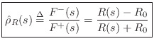
Calculate the reflectance of the terminated waveguide. That is, find the Laplace transform of the return wave divided by the Laplace transform of the input wave going into the waveguide. In general, the reflectance of an impedance step for force waves (voltage waves in the electrical case) is
This is easily derived from continuity constraints across the junction. Specifically, referring to Fig.F.1b, let

By the definition of wave impedance in a waveguide, we have
Thus,
![\begin{eqnarray*}
0 &=& V(s) + V_R(s)\\
&=& \left[V^{+}(s)+V^{-}(s)\right] + ...
...s)}\right]
&=& \frac{2}{R_0}F^{+}(s) + \frac{2}{R(s)}F^{+}_R(s)
\end{eqnarray*}](http://www.dsprelated.com/josimages_new/pasp/img4758.png)
Defining
![]() and
and
![]() , we have
, we have
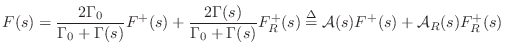
Now that we've solved for the junction force
Finally, the force-wave reflectance of an impedance step from
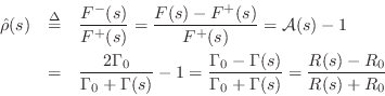
as claimed.
Reflectances of Elementary Impedances
We now derive the reflectances of the elements used in LTI analog electric circuits, viz., the capacitor, inductor, and resistor.
Capacitor Reflectance
For a capacitor of ![]() Farads, the driving-point impedance is (see
§7.1.3)
Farads, the driving-point impedance is (see
§7.1.3)
Inductor Reflectance
For an inductor of ![]() Henrys, we have
Henrys, we have
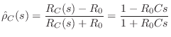
Resistor Reflectance
Finally, for a resistor of ![]() Ohms, we get
Ohms, we get
Note that both the capacitor and inductor reflectances are
stable allpass filters, as they must be. Also, the resistor
reflectance is always less than 1, no matter what waveguide impedance
![]() we choose.
we choose.
Choosing Impedance to Simplify Element Reflectance
Observe that there is a natural choice for each waveguide impedance which will give us a normalized, ``universal reflectance'' for each element:
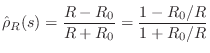
- For the capacitor, setting
 gives
gives
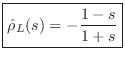
- For the inductor, setting
 gives
gives
- And for the resistor, we set
 to obtain

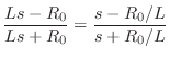
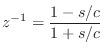
Digitizing Elementary Reflectances by Bilinear Transform
Going to discrete time via the bilinear transform means making the substitution
 |
(F.11) |
where
Solving for ![]() gives us the inverse bilinear transform:
gives us the inverse bilinear transform:
In this case, we see that setting ![]() further simplifies our
universal reflectances in the digital domain:
further simplifies our
universal reflectances in the digital domain:
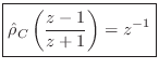
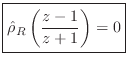
- For the ``wave digital capacitor'' (or spring), Eq.
 (F.8) becomes
- For the ``wave digital inductor'' (or mass), Eq.(F.9) becomes
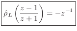
- And for the ``wave digital resistor'' (or dashpot), Eq.(F.10) becomes
as before in the continuous-time case.
Note that this choice of ![]() is also the only one that eliminates
delay-free paths in the fundamental elements. This allows them to
be used as building blocks for explicit finite difference
schemes.
is also the only one that eliminates
delay-free paths in the fundamental elements. This allows them to
be used as building blocks for explicit finite difference
schemes.
We may still obtain the above results using the more typical value
![]() (instead of
(instead of ![]() ) in the bilinear transform. From
Eq.
) in the bilinear transform. From
Eq.![]() (F.12), it is clear that changing
(F.12), it is clear that changing ![]() amounts to a linear
frequency scaling of
amounts to a linear
frequency scaling of ![]() . Such a scaling may be compensated
by choosing the waveguide (port) impedances to be
. Such a scaling may be compensated
by choosing the waveguide (port) impedances to be
![]() (instead of
(instead of ![]() ) for the inductor, and
) for the inductor, and
![]() (instead of
(instead of
![]() ) for the capacitor.
) for the capacitor.
Next Section:
Summary of Wave Digital Elements
Previous Section:
State Space Summary