


Design of an anti-aliasing filter for a DAC
Overview
- Octaveforge / Matlab design script. Download: here
- weighted numerical optimization of Laplace-domain transfer function
- linear-phase design, optimizes vector error (magnitude and phase)
- design process calculates and corrects group delay internally
- includes sinc() response of the sample-and-hold stage in the ADC
- optionally includes multiplierless FIR filter
Problem
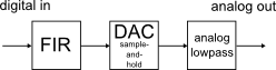
Figure 1: Typical FIR-DAC-analog lowpass line-up
Digital-to-analog conversion connects digital signal processing with the analog world (Fig. 1). For audio frequency signals, it is not difficult to find a ready-made solution, but in other applications, it usually needs to be designed individually, especially if high performance or low cost need to be achieved.
A digital-to-analog converter generates a stairstep response from its input samples that includes aliases of the signal at multiples of the sampling rate. These aliases need to be removed with an analog filter.
Usually the anti-aliasing filter is designed mainly for the required alias rejection, where some deterioration of signal quality in the passband is accepted. It is corrected with a digital equalizer prior to the AD conversion.
A popular approach to equalization - also of the sinc-shaped frequency response of the DAC itself - is a FIR filter with powers of two for non-zero coefficients. Such a filter can be implemented efficiently in hardware with bit shift operations, whereas a conventional multiplier-based equalization filter would be impractical due to the high sampling rate.
As the digital filter allows for example to pre-emphasize high frequencies, there is no direct need to use a 'flat' textbook prototype for the analog filter (i.e Butterworth, Bessel, Chebyshev), removing one design constraint. Instead, a possible strategy is for example to avoid high Q poles at high frequencies, as they are the hardest to implement.
Matlab / Octaveforge code
The program implements a numerical optimization of an analog filter for linear phase and an arbitrary magnitude response.
As is common in digital filter design, the requirements are stated using a nominal frequency response and a weighting vector.
The objective function that is called by the optimizer calculates the frequency response of the designed filter, in combination with other (fixed) frequency responses, such as those of the sample-and-hold stage and the FIR filter. It determines and compensates the group delay, calculates the complex-valued error relative to the ideal frequency response, and combines it with the weighting vector into an error metric that is given back to the optimizer.
Optionally, the design process can include a multiplier-less FIR equalizer, and it can be iterated for all possible equalizers (exhaustive search).
Some 'housekeeping functions' are included for convenience so that optimization variables can be added or removed by changing a single line of code.
Least-squares design
A weighted least-squares design, as presented, has the freedom to leave more error at frequencies where the improvement is more difficult. If the problem allows, this philosophy will achieve better performance than a min-max (Chebyshev norm) design for noise-like signal, such as communications channels, where the overall error averages over all passband frequencies.
But there is no guarantee that any single frequency point will pass some requirement. If such a min-max design is needed, the frequency-dependent weights could be adjusted proportionally to a margin to some requirement, a method known as 'iterative reweighted least squares' (IRLS).
An example for an IRLS outer loop can be found here.
Example
The example in the code suppresses the alias of a WCDMA channel sampled at ten times the chiprate (38.4 Msps), for example in a cell phone transmitter.
The numbers aren't very realistic, this is a made-up example.
Analog filter only (no FIR)
Figure 2 shows the output if the digital FIR filter is disabled.
Traces:
- weight: The weight vector, as seen by the objective function
- sinc: The frequency response of the DAC sample-and-hold stage
- FIR: FIR filter (disabled)
- p1: analog filter, real-valued pole
- p2: analog filter, resonant pole pair
- combined: system response
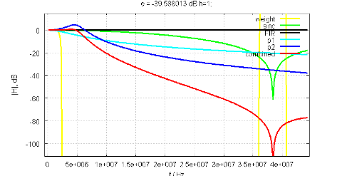
Figure 2: Filter design without FIR
Analog filter designed with FIR equalizer
In Figure 3, the analog filter was redesigned in combination with a [-1, 2, 2, -2] FIR filter.
The error (objective function value) has improved by 5.4 dB.
Thanks to the digital pre-emphasis, the Q factor of the resonant pole pair in the analog filter reduces from 1.6 to 0.7, which allows for an easier implementation.
While the peaking of the FIR frequency response may seem problematic, it occurs at frequencies where there should be only negligible energy in the digital signal. At the edge of the wanted signal, about 3 dB additional headroom appear to be necessary.
Increased digital noise boosting is largely compensated by the analog filter, whose gain at high frequencies is now lower. There is some overall small increase at 15 MHz, as it is a "don't-care" region in the design example.
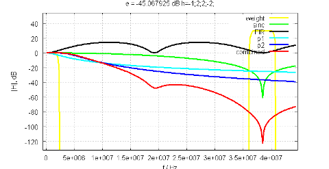
Figure 3: Filter design using [-1, 2, 2, -2] FIR at 1/4 output rate
Download
The program can be downloaded here .
It was developed on OctaveForge, and works on Matlab too (with toolboxes).


- Comments
- Write a Comment Select to add a comment
To post reply to a comment, click on the 'reply' button attached to each comment. To post a new comment (not a reply to a comment) check out the 'Write a Comment' tab at the top of the comments.
Please login (on the right) if you already have an account on this platform.
Otherwise, please use this form to register (free) an join one of the largest online community for Electrical/Embedded/DSP/FPGA/ML engineers:


