Analog-to-Digital Confusion: Pitfalls of Driving an ADC
Imagine the following scenario:
You're a successful engineer (sounds nice, doesn't it!) working on a project with three or four circuit boards. More than even you can handle, so you give one of them over to your coworker Wayne to design. Wayne graduated two years ago from college. He's smart, he's a quick learner, and he's really fast at designing schematics and laying out circuit boards. It's just that sometimes he takes some shortcuts... but in this case the circuit board is just something to digitize some thermistor measurements -- he says he's putting on a microcontroller with a built-in analog-to-digital converter, which will then send the measurements to the rest of the system via a CAN bus. What could go wrong?
"Well, I've got two ADC channels for thermistors, and a third one sensing 1.8V. It works fine," he says, "except... well, it's the funniest thing. I heat up one channel's input from 0 degrees C to 100 degrees C, and the measurements are what I expect... but the other channel increases in temperature by about 10 degrees."
You offer to give him a hand, but he says he'll come see you after he does some more investigating.
Later he drops by. "I don't get it," he says. "The first channel affects the second one, but then I heated up the second channel's input from 0 degrees C to 100 degrees C, and it doesn't affect the first. But they're the same circuit!"
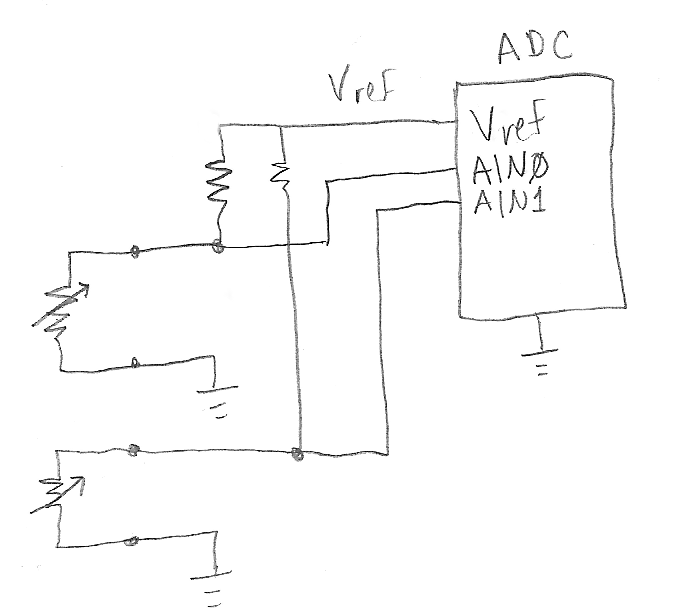
Here's the relevant part of Wayne's design (a third channel AIN2 sensing a voltage is not shown):
What's going on?
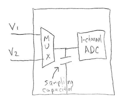
Well, the first thing to know is what the analog-to-digital converter looks like electrically. Most multichannel sampling ADCs are really just a combination of an analog multiplexer, a small sample-and-hold capacitor, and one ADC. They connect the capacitor to the selected input channel for a brief period of time (the sampling time), and then connect the capacitor to the ADC to digitize the capacitor voltage (the conversion time).
The sampling capacitor sees different voltages from one channel to the next, and during its sampling time, the capacitor has to charge/discharge from its previous voltage to the voltage it's supposed to have. So there's a certain maximum source impedance you have to provide to the ADC. If you use a high-resistance voltage divider, at the end of the sampling time, the capacitor will not completely charge to the voltage you intended, and instead, it will retain a voltage that is influenced by its previous voltage.
Let's throw some numbers here.
Suppose the sampling capacitor is 10pF, your voltage divider has 100K output impedance, and the sampling time is 1usec. The RC time constant in the sampling capacitor is 1usec. The important calculation here is K = e-T/RC which in this case is K = 0.368. The voltage seen at the end of the sampling time = (K * previous voltage) + (1-K) * intended voltage -- you're measuring 63.2% of the voltage you intended, and 36.8% of the old voltage.
Not good!
If you can increase the sampling time, you can alleviate this situation. For T = 2usec, K = 13.5%, so that's still a lot. You generally want to make sure that K is less than 1/2 LSB of the ADC, so that the effect is minimal. For a 10-bit ADC, that translates into T = about 7.6*tau. (12-bit: 9tau; 8-bit: 6.2tau; 14-bit: 10.4tau; 16-bit: 11.8tau)
That's one way to solve the problem. The other way is to use an external capacitor as a charge reservoir.
Thought experiment:
Suppose you have a capacitor C1 charged to a voltage V1, and you have a capacitor C2 charged to a voltage V2, and you connect the two in parallel. What's the voltage Vfinal after you connect them?
Well, you have a total charge Q = C1*V1+C2*V2, and a net capacitance Cfinal = C1 + C2, so Vfinal = Q/Cfinal = (C1*V1+C2*V2)/(C1+C2).
Again, let's throw in some numbers.
The sampling capacitor is C1=10pF, and it's at V1 = 1V. An external capacitor C2 = 0.01uF = 10000pF is at 0V. The end voltage is (10pf*1V)/(10pF+10000pF) = 1mV. Connecting a small sampling capacitor to an external capacitor that is 1000 times larger will change the external capacitor's voltage by 1/1000 of the difference between the initial voltages. (This is true in general for any ratio K that's much larger than 1.)
The upside of this approach is that the external capacitor automatically charges up the sampling capacitor and is barely affected by the switching transient. The downside is that the time constant for it to recharge to its original value is much longer: the voltage divider still has 100K output impedance, but now C = 0.01uF so tau = 1 millisecond.
For this approach to work, you have to make sure the charge reservoir capacitor is large enough so that the transient caused by its connection to the sampling capacitor is small, usually less than 1/2LSB of the ADC. For a 10-bit ADC, that means the external capacitor should be 2048 times larger than the sampling capacitor (for 12-bit the ratio is 8192, for 14-bit, 32768, and for 16-bit, 131072).
With a large external charge reservoir capacitor, you can use short sampling times.
After a discussion with Wayne on the subject, he decides to add a charge reservoir capacitor, and goes back to the lab to try it. An hour later he comes back.
"I put a 0.1uF capacitor across each of the ADC inputs, and that helped somewhat, but it still has the same problem; the second measurement gets affected slightly by the first one."
"What sample rate are you using?" you ask. "Not the sample rate between samples, but the rate at which you repeat sampling the entire sequence of channels."
"10kHz," he says.
"Aha, there's your problem."
Let's look at the sampling capacitor again. Suppose the ADC runs from 0 to Vref, and one channel is at V1 and the next one is at V2. The capacitor needs to be charged up by its input; the electrical charge Q transferred = C*(V2-V1), where C is the sampling capacitance. This happens not just once but every time it is sampled; if the sampling frequency is f, then the rate at which charge is transfered is C*deltaV*f. This is a current, that presents itself as impulses or "gulps" of charge C*deltaV, but the average current is C*deltaV*f. This is true no matter what external capacitor is used.
When the circuit driving the sampling capacitor is a voltage divider with output resistance R, then the voltage divider's output node sees an average voltage drop of R times this current, or R*C*deltaV*f.
Without an external capacitor, this happens only during the switching transient, and if you wait the 8-12 time constants until the voltage settles back down, then you see the proper voltage. But if you add an external capacitor to keep the transients small, then it low-pass filters the voltage and there's no way to avoid the voltage drop -- which is proportional to the voltage difference between channels, so it is unpredictable and time-varying.
Again, some numbers:
C = 10pF, deltaV = 3V, R = 100K, f = 10kHz. The average voltage drop is 0.03V, or deltaV * 1%.
This amount is higher (and therefore worse) when the sampling capacitance is higher, or the external impedance is higher, or the repeat rate is faster.
Fast sampling is your enemy here. If you want to use high-impedance voltage sources with an ADC, you have to either avoid external capacitance and use long sampling times to wait for the sampling capacitor to settle, or use external capacitance intentionally but avoid fast sampling repeat rates. (High impedance voltage sources are bad for another reason: ADCs usually specify their input leakage current, which is separate from this charge-transferring current, but it also can cause a voltage drop.)
You discuss this with Wayne.
"So I have to put an op-amp to buffer the voltage?" he asks.
"Well, basically, yes, if you want to sample fast, that is. You could sample more slowly, you know."
"Yeah, but I want to do oversampling and filtering in software. Besides, it sounds like I should probably have the op-amp in there anyway."
"Good thinking. There's one more problem you should know about, though...."
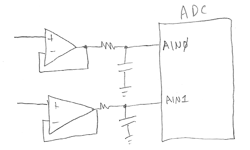
So you buffer your voltage divider with an op-amp and connect that to the ADC input. The problem with op-amps is that they like to see "nice" (i.e. resistive) electrical loads, and if you whack their output by connecting and disconnecting a capacitor, there's not really a good guarantee of how long the op-amp will settle down to a buffered version of the voltage divider. Remember, the sampling capacitor wants a fast gulp of charge. For example, if you want a 1 microsecond settling time, and the sampling capacitor is 10pf, and needs to change from 0V to 3V, then the current during this period is Q/T = CV/T = 30uA. That's not that much for the op-amp to deliver, but the dynamics need to be fast and aren't specified in op-amp datasheets -- they typically spec what happens when you put voltage transients on the op-amp input, which is a completely different situation from a fast change in output load. In any case, for a 1 microsecond settling time you'll need more than a 1MHz gain-bandwidth op-amp, probably one in the 10-20MHz range at least.
The best way to deal with this is to put a simple RC filter on the op-amp output. Pick an R and C so that by the end of the sampling period, the sampling capacitor has settled to within 1/2 an LSB of its final value. But you also need to make sure there's enough resistance R so that the op-amp is stable. Many op-amps aren't stable with excessive capacitive loads. I usually find that something around R = 499 ohms, C = 470pF will work fine. That creates a time constant of about a quarter-microsecond, and adds enough external capacitance so that it delivers most of the charge needed by the sampling capacitor, and keeps the op-amp from having to do so. And *please* remember when you get to circuit board layout to place the external capacitance as close as possible to the ADC.
This is a trade-off for driving ADC inputs: if you want the time between sampling input channels to be very short (i.e. finish an ADC sampling sequence quickly), you have to add a buffer and an RC filter on the ADC input. If you don't want to have to go to the trouble to do so, you can't expect to sample at a fast rate, and you need to do the analysis to make sure you're not introducing cross-coupling from one channel to another.


- Comments
- Write a Comment Select to add a comment
Hope all is well, but looking at Wayne's circuits I was mortified to see he was driving the thermistors directly from the vref supply my experience with most micro-controllers and their ADC circuits is that only the micro vref lines should only be a small filter cap(but this is dependent on the type of micro) ,I do not beleive it is something anyone should supply current to drive a variable load(thermistor) or for that matter any type of load... I think a more suitable solution would be to buffer the vref line into a voltage follower opamp to supply the thermistors... This way the change in the thermistor will not effect vref thereby affecting adc conversions. That been said I do agree with the rest of what you stated but I see this loading of the vref line as real issue problem... again this maybe more brand/type dependent of the micro.
Unless it is a safety margin, maybe taking into account other inherent ADC errors.
Hello Jason,
Could you please explain why the external capacitance must be as close as possible to the ADC? Currently I'm working with a STM32 microcontroller which ADC is connected to a buffer, exactly the same way you show in the last picture, but in the board the capacitance is far from the ADC. I don't know if this is the reason why I have to put a delay before reading the ADC (equivalent to 10 times RC) to get the same value as measured with the voltmeter.
Thanks!
Marco

Could you please explain why the external capacitance must be as close as possible to the ADC?
Good question! There are two reasons that have to do with the circuit board traces between the capacitor and the ADC:
- There is always some impedance between the external capacitance and the ADC itself, due to the circuit board trace. Traces have parasitic resistance and inductance, and both of them prevent the capacitors from providing the needed charge storage for the ADC.
- Long traces can act as antennas that pick up electrical noise
The noise effect is hard to model, and unless you really had long traces (>30cm), and no ground plane, you probably wouldn't notice.
For the impedance, you should be able to figure out the parasitic R and L of the trace by knowing the length and width of the trace, and the thickness of copper. (Many PCB software packages will calculate this for you.) These form a series RLC circuit, and as long as the time constants of the RLC circuit are much shorter than the ADC sampling time, you don't need to worry about the parasitic impedance. But if the R and L are large enough, then the ADC sampling time will not be sufficient.
Next time make sure your board layout places these close to the ADC. Within 2-3 centimeters is probably good enough, but closer is better.
Thanks for your answer Jason. I have two additional questions:
- I'm using four channels of the ADC and for a sampling time of 1.5 cycles I always get correct values for channels 1, 2 and 4 but for channel 3 I get a value higher than expected (as the example you explained), the fact that the sensor connected to channel 3 is farther than the others (around 5 cm far away from the ADC port) could be a reason to this behaviour ?
- I arrive to solve this problem by increasing the sampling time, but if I increase it to the maximum possible the ADC returns very high values. Could this be because I'm waiting so long that the ADC's sampling capacitor gets charged with the voltage of more than one ADC channel?
Thanks!
Marco
Hi Jason,
I need your in advice with using SDADC. I am using a STM32F37x/38x that has 3 Sigma Delta ADC for thermistor, RTD and voltage measurement. I am using the 1st and 3rd SDADC converters in Single ended zero reference mode. No matter what Op Amps or input capacitor sizes or input resistors I use after startup and offset calibration data stored both configuration registers is all over the place. Every time I power up the STM I get different offset values stored in the configuration registers. The SDADC embedded in STM32F37x/38x devices provides automatic offset calibration by shorting internally both channel inputs (positive and negative), perform conversion and store result in internal register (configuration register) and the subtract automatically the calibration value from conversion value during standard conversion. The capacitors used are 10uF (the same value used in the STM Eval board) and they extremely closed to the SDADC. I have tried lower values like the ones for SAR ADCs and the results are even worse. Also tried both 1.5 and 6 MHz sampling clock frequencies. Also I am using 5 channels on the first SDADC and 3 on the third. Measurements on one SDADC channel are affected by the other channels of the same SDADC. This leads my to believe that the internal capacitor of the SDADC is not charging properly. The ADC input internal cap is around 0.659pF for gain 1 and 1.759pF for gain 8. How is it possible that this capacitors do not charge properly. Can you give some hint of where I should look to fix this problem.
Your article about the ADC is awesome.
Thank again,
Mike
Sorry, I can't help you; nothing obvious comes to mind. I suggest you contact ST to get technical support.
Jason,
Reopening what seems to be an old discussion. I have a project with multiple thermistors measuring different temperature points that runs on a RPI3. My board the RPI sits on uses the MCP3008 as the ADC. My initial design was extremely basic and I was seeing that one probe was very accurate and as I turned on even one more probe they seemed to couple together and an action by one had a direct affect on the other even to the point of them being exactly the same. I fought with the SPI max_speed value programmatically but nothing removed the coupling. Then I found this post you made. I had already tried step one by reducing the max speed on the SPI and also putting in 100 ms delays between each reading. So I redid my board with OpAmps and RC filters on the back end as you describe. Things improved... slightly. With the second probe it seemed to not couple until the temperature shift on it was fast (putting it into a mug of hot water) [and yes it is a waterproof probe]. Then I add a third and the first and third couple and the second works properly. I then add a 4th and the first and second seem to be fine with the 3rd and 4th coupled. To make matters even more odd, If I just use a multimeter to take a reading at each input pin on the MCP3008 the voltages are all as they should be and the software works for a short while after I take readings and then it goes back to coupling. Do you have any ideas on what could possibly be causing this?
To post reply to a comment, click on the 'reply' button attached to each comment. To post a new comment (not a reply to a comment) check out the 'Write a Comment' tab at the top of the comments.
Please login (on the right) if you already have an account on this platform.
Otherwise, please use this form to register (free) an join one of the largest online community for Electrical/Embedded/DSP/FPGA/ML engineers: