Welcome back! Today we’re going to zoom around again in some odd directions, and give a roundabout introduction to the semiconductor industry, touching on some of the following questions:
- How do semiconductors get designed and manufactured?
- What is the business of semiconductor manufacturing like?
- What are the different types of semiconductors, and how does that affect the business model of these manufacturers?
- How has the semiconductor industry evolved over time?
- How do semiconductor manufacturers approach risk-taking in their strategic decisions?
This last question on risk-taking is especially relevant to the chip shortage, because semiconductor manufacturing involves a lot of expensive, high-stakes decisions with consequences that arise several years later — something that influences the choice of how much manufacturing capacity to build. (Robert Palmer, a member of AMD’s Board of Directors, allegedly compared building semiconductor fabs to Russian roulette: “You pull the trigger, and four years later you learn whether you blew your brains out or not.”)
In part one of this series, I talked about how bad the chip shortage is, I presented a two-minute summary of some of the factors that led to the chip shortage, and I gave a sneak preview of some of its nuances. We looked at toilet paper shortages. And played Lemonade Stand. Yes, really.
Part two’s focus is mostly centered around a kind of 1980s-1990s “retro” theme. If you don’t remember the USSR, the Berlin Wall, Yugoslavia, or parachute pants, consider this a history lesson of sorts.
Every good history of Silicon Valley starts with how William Shockley left AT&T’s Bell Laboratories, where he co-invented the first working transistor with John Bardeen and Walter Brattain in 1947, to start Shockley Semiconductor, located in a Quonset hut in Mountain View, California, in 1956, and how the Traitorous Eight left Shockley Semiconductor and started Fairchild Semiconductor in 1957 with a secret meeting in the Clift Hotel, where they signed dollar bills as a symbolic contract.
This is not that kind of history.
Think of it, instead, as a sort of magical journey with an invisible, attention-span-deficient Ghost of Semiconductor Past, starting in 1983 — ooh, look, there’s Huey Lewis and Cyndi Lauper! — and bouncing around among the past few decades. A set of hyperactive case studies, in a matter of speaking. (This is a long article. A very, VERY LONG article — no, you don’t understand; I’ve written long articles before, but this is a record for me — which I hope is worth the time needed to read it. It could probably be four or five articles instead, but I have my reasons for not splitting it up.) We’ll be covering these sorts of topics:
- some impacts of the prevailing customer market from around 1975-1985, during the Microcomputer Revolution
- the value (or lack thereof) of certain media commentary on the chip shortage
- an introduction to semiconductor fabrication with MOS Technology and Commodore
- some concepts of microeconomics
- capital expenditures
- the history and economics of DRAM manufacturing
- purchases of new and used semiconductor fabrication plants
But first, back to 1983. Why 1983? I have some personal reasons — for example, I first played Lemonade Stand in the fall of 1983 — but, more importantly, that year marked a major turning point in the rise of the personal computer. There are two pieces of evidence I’d like to share: a quantitative graph, and one little excerpt from a newspaper article of the time.
Interlude, 1983: A Brief Introduction to the Microcomputer Revolution and the Semiconductor Industry
The graph is from Jeremy Reimer’s excellent writeup of three decades of the personal computer industry in Ars Technica in 2005. The sales growth of the Commodore 64 and IBM PC in 1983 was just insane. (Go read the whole piece if you have time.)

The excerpt is from an article in the December 10, 1983 issue of the New York Times, titled Under 1983 Christmas Tree, Expect the Home Computer:
This is the year in which the home computer will join the sled and the bicycle under the Christmas tree.
In numbers that outstrip even the most optimistic predictions, Commodores, Ataris and Colecos are being snapped up from the shelves. Americans have embraced the home computer as their favorite gadget for a Christmas present, replacing the food processors and video games of Christmases past.
“Last year, computers were new, unique and expensive,” said Egil Juliussen, president of Future Computing Inc., a market forecasting concern that expects 2.5 million home computers to be sold this Christmas, twice as many as last year. “This year, they’re cheap, and they have become the gift.”
Only six months ago, a fierce price war erupted among home computer manufacturers, sending many into a tailspin from which it appeared some would not recover. This year, the industry will lose almost \$1 billion.
Price War Aids Consumers
But the same price war that badly hurt the industry has brought home computers within the reach of millions of families. At the same time, industry advertising has helped make people feel more comfortable with the notion of a computer in their home or, alternatively, apprehensive that their children will fail without them. Suddenly, the home computer glut has given way to a shortage.
So there you have it. Boom! Home computer explosion. Gluts and shortages. Sounds familiar.
1983 began with Time Magazine’s January 3, 1983 “Man of the Year” issue dedicated to the computer. This issue contained a special section on computers, including a feature titled The Computer Moves In along with articles on programming and a computer glossary. While the Man of the Year title (actually Machine of the Year) was judged based on the status at the end of 1982, I really think of 1983 as the Year of the Personal Computer. Sure, the preceding years each brought new and exciting developments:
- 1977: the Apple II, the TRS-80, the Commodore PET, and the Atari VCS
- 1978: the Intel 8086 processor and Space Invaders
- 1979: the Atari 400 and 800 and TI-99/4
- 1980: Pac-Man and the Sinclair ZX-80 and Commodore VIC-20
- 1981: the IBM PC and the arcade game Donkey Kong
- 1982: the Intel 80286 processor and Commodore 64
There was certainly a sense that The Future Is Here! and articles in various magazines and newspapers heralded a new age of technology. The New York Times had an article in December 1978 predicting that “The long‐predicted convergence of such consumer electronic products as television sets, videotape recorders, video games, stereo sound systems and the coming video‐disk machines into a computer‐based home information‐entertainment center is getting closer.”
But I stand by my choice of 1983 as the year that personal computers really took off, both in an economic and cultural sense. Here are a few other reasons:
-
The movie WarGames came out in summer 1983, and with the later September 5, 1983 issue of Newsweek about Neal Patrick and the Milwaukee 414s, we were all introduced to the subculture of “hackers”.
-
Compute’s Gazette began publication, bringing articles and free software (to those willing to type it in from code listings) to Commodore computer owners, as a spinoff of Compute! Magazine. As it explained in its premier issue:
Where is the demand coming from? Well, we estimate that Commodore is currently selling over 100,000 VIC-20s and 64s a month. Dozens of software and other support vendors are rushing to supply products for these rapidly growing markets. Personal computing power is now expanding at a rate far past that predicted by industry observers. With the recent price decreases in the VIC-20 and 64, we expect this trend to continue its dynamic escalation.
-
Electronic Arts published its first games in 1983; we’ll take a closer look at one of them.
-
In summer 1983 I went to a “computer camp” for a week where we got to try out programming with VIC-20 computers and saw WarGames at the movie theater. Later that year, my family bought a Commodore 64. (Like I said, personal reasons. Okay, you don’t really care about either of those events, but they made a big impression on me.)
-
The video game crash of 1983 resulted from a tidal wave of interest in hardware and software companies racing to fill a mass demand for video games in the United States. It got filled, all right. Price wars dropped the cost of video game consoles and low-end computers like the Commodore 64 to the point where they were more affordable — good for consumers, but bad for the manufacturers. Atari was one of the most heavily-hit companies, with so many unsold games and consoles that they actually buried this excess inventory in a New Mexico landfill. The glut devastated the video game console market for two years, until the 1985 release of the Nintendo Entertainment System — and was almost entirely predictable. As Wikipedia states:
Each new console had its own library of games produced exclusively by the console maker, while the Atari VCS also had a large selection of titles produced by third-party developers. In 1982, analysts marked trends of saturation, mentioning that the amount of new software coming in would only allow a few big hits, that retailers had devoted too much floor space to systems, and that price drops for home computers could result in an industry shakeup.
In addition, the rapid growth of the videogame industry led to an increased demand, which the manufacturers over-projected. In 1983, an analyst for Goldman Sachs stated the demand for video games was up 100% from the previous, but the manufacturing output had increased by 175%, creating a significant surplus. Atari CEO Raymond Kassar recognized in 1982 that the industry’s saturation point was imminent. However, Kassar expected this to occur when about half of American households had a video game console. Unfortunately, the crash occurred when about 15 million machines had been sold, which soundly under-shot Kassar’s estimate.
Oddly enough, in 1983 there was a semiconductor shortage:
Demand, which has picked up sharply in recent months mostly because of the boom in personal computers, is now exceeding supply for most kinds of silicon chips used in computers, telecommunications equipment and other electronic devices.
At a conference here, industry executives said customers had to wait as much as 20 weeks or more for delivery of their orders. On the one hand, the shortage is a blessing for the companies, which are selling all they can make. Price-cutting has ended, profits are improving, and company stock prices have risen.
Both gluts and shortages have related dynamics, which are relevant to understanding this year’s semiconductor shortage. The computer and semiconductor industries are both examples of cyclical industries, which undergo boom and bust periods somewhat akin to oscillations in an underdamped, marginally stable control system.
Why do we get these sort of business instabilities, especially in the high-tech world, and especially if we can see them coming? Part of the answer comes from time delays, and part of it from corporate motivation to manage the pain of capital expenditures, something that becomes very clear if you look at the business of DRAM (dynamic RAM).
Disclaimers
I need to get through a few disclaimers:
I am not an economist. I am also not directly involved in the semiconductor manufacturing process. So take my “wisdom” with a grain of salt. I have made reasonable attempts to understand some of the nuances of the semiconductor industry that are relevant to the chip shortage, but I expect that understanding is imperfect. At any rate, I would appreciate any feedback to correct errors in this series of articles.
Though I work for Microchip Technology, Inc. as an application engineer, the views and opinions expressed in this article are my own and are not representative of my employer. Furthermore, although from time to time I do have some exposure to internal financial and operations details of a semiconductor manufacturer, that exposure is minimal and outside my normal job responsibilities, and I have taken great care in this article not to reveal what little proprietary business information I do know. Any specific financial or strategic information I mention about Microchip in these articles is specifically cited from public financial statements or press releases.
There you go; you’ve been informed.
One other topic I want to cover, before returning to the early days of computing, is some recent gossip, to remind us of a few very important points.
Interlude, 2021: Tech Gossip (Blame, Excuses, Prognostication, and Silver Bullets)
It’s always interesting to hear What Some People Say about the chip shortage… bad news is a time when everyone gets to weigh in on the topic, like a relative repeating gossip at a funeral. (“Oh, I heard he wrote Jimmy out of his will for dating his ex-wife, such a shame, if only he’d cut back with the cigarettes maybe he would have beat the cancer.”)
There is a lot of this sort of thing in the news lately. You need to realize that no one has a satisfying answer, so in a vacuum, here’s what we get instead, a superficial coverage of the problem that touches on half-truths, wishful thinking, and speculation.
Pat Says
Intel’s CEO, Pat Gelsinger, was quoted in an article in Fortune titled “Chipmakers to carmakers: Time to get out of the semiconductor Stone Age” that automotive manufacturers should be making ICs on more modern technology processes:
“I’ll make them as many Intel 16 [nanometer] chips as they want,” Intel chief executive Pat Gelsinger told Fortune last week during his visit to an auto industry trade show in Germany.
Carmakers have bombarded him with requests to invest in brand-new production capacity for semiconductors featuring designs that, at best, were state of the art when the first Apple iPhone launched.
“It just makes no economic or strategic sense,” said Gelsinger, who came to the auto show to convince carmakers they need to let go of the distant past. “Rather than spending billions on new ‘old’ fabs, let’s spend millions to help migrate designs to modern ones.”
And in his keynote speech at that IAA Mobility trade show: (at 17:50)
I’m also excited today to announce our Intel Foundry Services. In March of this year, I announced IDM 2.0 that we are foundering our products, but we’re also opening wide the doors of Intel to be a foundry for others’ products as well. Today, we’re announcing the European foundry services at Intel 16 and other nodes out of our Ireland facility. And we believe this has an opportunity to help expedite the end to this supply shortage, and we’re engaging with auto and other industries to help build on those, uh, capabilities.
But I’d also say some might argue, well, let’s go build… most of those auto chips are on old nodes. Don’t we need some old fabs for old nodes? Do we want to invest in our past or do we want to invest in the future? A new fab takes four or five years to build and have production-worthy.
Not an option to solve today’s crisis. Invest in the future, don’t invest backwards. Instead, we should be migrating old designs onto new, more modern nodes, setting them up for increased supply and flexibility into the future.
Lisa Says
AMD’s CEO, Lisa Su, said in an interview at Code Conference 2021
If you think about the semiconductor industry, we’ve always gone through cycles of ups and downs where, you know, demand has exceeded supply or vice versa. This time it’s different. And what’s different this time is every industry needs more, and so, you know, the confluence of that means that there is a, there is an imbalance. I will say that there’s a tremendous amount of investment going in, so, uh, there are, you know, over 20 new factories are coming online this year… and, and, you know, 20 more, you know, 20+ more in… um… uh… in planning and, um, so it’s still gonna be tight, you know, this year’s tight, first half of next year likely tight, but it’ll get better, as we get into 2022.
…
… we’ve seen, um, some stuff about automotive shortages ‘cause there were some supply chain interruptions there, so— It’s just every market has seen the demand go up, and um, and the key here with these complex supply chains is you may need thousands of chips, you know, only one of them being short is going to cause you to not ship your system, and so there’s just a lot of, let’s call it, um, mixing and matching of, of these things… But— you know, what I will say is, it will be solved. Okay, we, heh, [chuckling] the semiconductor industry has been through these things and it, it will absolutely, um, you know, uh, normalize, uh, supply to demand.
[Kara Swisher, host, interrupting] And when do you expect that to happen?
[Su] Uh, I would say it gets better next year. You know, not, not, um, not immediately, but it will gradually get better, as, uh, more and more plants come up, and it takes, you know, we’re an industry that just takes a long time to get anything done, so, you know, it might take, you know, 18 to 24 months to put on a new plant, and in some cases even longer than that, and, so, you know, these investments were started, uh, perhaps a year ago, and so they’re, they’re coming online, you know, as we, as we go through, uh, the next couple of quarters.
Elon Says
Elon Musk said, in a tweet in August 2021:
Tesla makes cars for export in first half of quarter & for local market in second half.
As publicly disclosed, we are operating under extreme supply chain limitations regarding certain “standard” automotive chips.
Most problematic by far are Renesas & Bosch.
Musk also stated in Tesla’s Q4 2021 earnings call, when asked for some “color” on the supply chain situation — Wall Street analysts can never get enough color — near the end of the call:
Elon Musk: Well, last year was chip hell of many chips, uh, so, silicon carbide inverters — were certainly one of them, but, uh, um —
Drew Baglino (Senior VP, Powertrain and Energy Engineering): Honestly, there’s a lot of annoying very boring parts.
Elon Musk: Yeah. It’s a ton of very simple control chips that, run-of-the-mill, literally, you know —
Drew Baglino: [Inaudible] you know.
Elon Musk: Yeah, basic chips to control.
Drew Baglino: Voltage references, oscillators, so they’re very boring things.
Elon Musk: Yeah, exactly. Like the little chip that allows you to move your seat back and forth. [Chuckling] That’s, actually, was a big problem.
Drew Baglino: Yeah.
Elon Musk: … the… couldn’t make seats. Um, so, I — like — but a lot of these things are alleviating. I think there’s, there’s some degree of the toilet paper problem as well, where, um, you know, the toilet paper shortage, uh, during COVID, and uh, like obviously it wasn’t really a, a suddenly, a, a tremendous enhanced need for ass wiping. Um, it’s just people panicked in order to — and got every paper product you probably, you could possibly wipe your ass with, basically. Um, and I wasn’t sure, is this like a real thing or not? I actually took my kids to the H-E-B and Walmart in Texas to just confirm that this was real.
Indeed, it was. Um, and there was, there’s plenty of food and everything else, but just nothing, no paper products, um, that didn’t cause a split up. So, um, an odd choice for people to panic about. Um, those, those things are — so, end of the world’s coming, I think toilet paper is the least of your problems.
Um, so, so, I think we, we saw just a lot of companies over-order chips, uh, and, and they buffer the chips, um, and so we should see — we are seeing alleviation in that… almost every area, but the output of the vehicle is — uh, goes with the, the least lucky, um, you know, um, what, whatever, whatever the most problematic item in the entire car is, and there’s like, at least, ten thousand unique parts in the car, so, uh, you know, way more than that if you go further up the supply chain, and it’s just — it’s just, which one is gonna be the least lucky one this time? It’s hard to say.
He Says That They Say That Somebody Says
Robert Carnevale wrote in a Windows Central article titled “The global chip shortage’s cause has been found — it boils down to one company, says report”
As reported by DigiTimes, some Taiwan-based tech manufacturers — think smartphones, PCs, and related gadgetry — have singled out Texas Instruments as being at the epicenter of the chip shortage’s widespread production pandemonium (via WinFuture). In case the name “Texas Instruments” sounds familiar to you, that’s because you very well may have used one of its calculators in your lifetime. That’s the company being accused of having a vice grip on global technology output.
This accusation is based on the fact that Texas Instruments manufactures analog chips that are essential for duties such as PC voltage regulation. Said chips are a fundamental part of much computing technology, and are in a more dire supply situation than the advanced, specialized chips the likes of TSMC and co. produce.
The aforementioned Taiwan-based sources say Texas Instruments’ inability to ramp up production capacity is the fundamental problem underpinning everything else. The question now is whether this supposed culprit identification will have any impact on the U.S. government’s shortage-combatting plans.
The DigiTimes articles — there are two of them, one mentioned above and another titled “Highlight of the Day: TI reportedly slow in expanding production”) — are behind paywalls now; I managed to stash the content from the Highlight of the Day article, back in November (and have faithfully reproduced its typographical errors here) for whatever it’s worth:
Pure-play foundry houses have been keen on expanding fab capacity, but the notebook industry continues to see serious chip shortage. Some industry sources are blaming Texas Instrument for its insuffcient supply. Networking device makers expect chip and component shortages will persist in 2022. But in the passive components sector, makers have seen demand slow demand.
IC shortage unlikely to ease until TI ramps up output: The global IC shortage is unlikely to ease until Texas Instruments scales up its output, according to sources in the notebook industry, which see supply-side constraints caused mainly by TI’s insufficient supply.
Enough of the Rumor Mill
There’s also Renée Says (Ampere’s Renée James: “I think what we thought was that we, I, I think this demand signal might have been read incorrectly in 2019 and 20 and in addition to that it uncovered, um, the fragility of the supply chain for semiconductors worldwide and the decline in U.S.-manufactured semis, which as you know is not just a supply chain issue, it’s also a national security issue for us, so, um, you know, one of the things that companies like mine, a small company, a startup only four years old, however I’ve been in this business for over 30 years, we know that there’s some systemic long-term things that we need to go after to build the health of U.S. semiconductors and that is what the Commerce Department is focused on talking with all of us about tomorrow and working on over the next five years. I mean, this is not a short-term thing, it’s something we need to get after as a national agenda.”) and Cristiano Says (Qualcomm’s Cristiano Amon: “I think in general, uh, everyone is complaining about, uh, the shortage of legacy technology and uh… but even those are gonna come online and uh… we’ll feel good about where we’re gonna be in 2022.”) and some others, but I’ve reached my limit.
This stuff is just frustrating to read, and I feel dirty repeating some of it, but I want to make a point: None of the tech gossip is really that useful.
Pat Gelsinger wants to help Intel sell its foundry services to the auto industry, and make them more resilient to capacity issues by manufacturing their ICs in fabs (Intel’s fabs, of course!) with newer technology which are seeing more investment — and we’ll talk about why that might or might not be useful in another article. Lisa Su is trying to paint a picture to reassure… but AMD doesn’t have any fabs, so it doesn’t control the situation directly; instead, it depends on foundries like TSMC to manufacture its processors. I trust she knows much more than I do about the situation, but at the same time, there’s no way to give a detailed answer without likely being wrong or sending messages to the financial world that can only get her or AMD into trouble. Elon Musk is rich enough that he can say what he wants and blame who he wants. If you want to learn something useful from CEOs, go listen to their company’s earnings calls and pay attention to concrete details that they are relating about their own company. If they’re talking about anyone else’s company, they’re no longer the expert.
As for the Windows Central and DigiTimes articles… bah!
I suppose there are shreds of truth in most of these sources, but you have to read enough in aggregate about the subject that you can distinguish the shreds of truth from what’s just a rumor, and unless there are supporting data or references to back up the assertions, they’re still just part of the rumor mill. Some say the chip shortage will be over soon, some say it will linger on; in fact, one day in mid-November of last year I spotted both back-to-back in my news feed:

The answers are all over the place. The uncertainty and confusion is enough to make you just throw up your hands in exasperation. What can you do?

I’ve been looking for good summaries of the situation for several months, and most of the time, whenever I think I’ve found something useful, in the same article or video there’s another detail that’s just totally out of left field and discredits the whole thing. Like a YouTube video (5 reasons why the world is running out of chips) that started off well, but then mentioned “minicontrollers” (are those just very large microcontrollers?) and towards the end slid into a lost-in-translation platitude that the chip-making industry “will need to keep innovating” and “will need to increase its capacity by working quicker, building square miles, and employing more people and machines.” Argh!!!

(If you do want some useful summaries, look at the links I listed near the beginning of Part 1.)
I’d like to leave the present gossip, and return to a historical look at earlier decades, instead of trying to explain today’s shortages directly. There are a few reasons. (Aside from the fact that today’s news is a bit demoralizing, whereas the 1970s and 1980s and 1990s exist at a safe, nostalgic distance.) One is that history tends to repeat itself, so we can look at a few of the past semiconductor business cycles, in their entirety, with the benefit of hindsight, instead of this mystery situation where no one really knows what is going to happen. The second is that the systems of the 1970s and 1980s are simpler to understand and explain. And the third is that I can actually find a lot of material on semiconductor history — there seems to be an unspoken statute of limitations on proprietary technology, so that if you’re an outsider and you want to know how today’s microcontrollers are designed, you’re out of luck, but people are willing to pull back the curtain and talk about the chips from the 1970s and 1980s, and all the crazy clever things they had to do to make them work.
So: the semiconductor industry. Yes.
Semiconductors! Meow!
I’m going to make the assumption that since this is on embeddedrelated.com, that you’ve worked with embedded systems, and so words like “op-amp” and “MOSFET” and “microcontroller” make sense to you. If not:
Semiconductors for People Who Are Not Electronics Enthusiasts
I think it would be easier for the average person to understand the semiconductor industry if it we just called it the microelectronics industry. “Semiconductor” makes people’s eyes glaze over, and just says something about the material these products are made of — something that conducts more than an insulator, but less than a conducting metal — not what they do, which is to control electrical signals. So there are a bunch of semiconductor manufacturers. They make chips, also known as “integrated circuits” (ICs), those little things in the black plastic packages that go in your phone or your computer. These things:

Close-up photograph of a dsPIC33CK Low Voltage Motor Control Board, taken by the author
Inside the chips are lots and lots of really small things called transistors that switch on and off and can be used to form microprocessors that run software and figure out how to get information from other computers through the air and display them on a screen as cat videos.
For most of this article, you won’t need to know anything about how chips actually work. (For the rest, you’ll just have to catch up or work around the jargon and technical details.)
Semiconductors for Electronics Enthusiasts
If you have worked on embedded systems, you’ve probably bought ICs and soldered them on circuit boards and read datasheets and schematics. Maybe even designed your own circuit boards.
You can make your whole way through a career just on that kind of information, without knowing much about what goes on inside a chip or how these manufacturers were able to make the chips, and just thinking of them as different brands of little black boxes. (I know, because I was one of those people during a good portion of my career, even after working at a semiconductor manufacturer for several years.)
If you stop thinking of the chip as a black box, and instead as a container for transistors, which has been manufactured in a factory and designed by a company which may be different than the one who owns the factory — well, then, things get a bit interesting. I think you should probably know something about these aspects, which I mentioned at the beginning of today’s article:
- How do semiconductors get designed and manufactured?
- What is the business of semiconductor manufacturing like?
- What are the different types of semiconductors, and how does that affect the business model of these manufacturers?
- How has the semiconductor business evolved over time?
- How do semiconductor manufacturers approach risk-taking in their strategic decisions?
Here’s a short version:
- Semiconductor ICs contain a “die” (sometimes more than one) which has been manufactured as part of a circular wafer.
- The surface of the die has been built up in a bunch of layers, using equipment that adds or removes materials selectively from parts of the die.
- Some of the layers are made out of semiconductors, usually altered in some way to change their electrical properties and form transistors.
- Other layers are made out of metal, forming lots of very small wires.
- The selective adding or subtracting usually happens with the help of photoresist that has been selectively exposed using light that shines through a glass mask. (The most cutting-edge process, EUV lithography, uses mirrors that bounce around ultraviolet radiation produced from tin plasma.)
- IC designers figure out what kind of transistors will fit on the die, how to hook them together, and how to test them. Nowadays everything is computerized, and specialized computer software called electronic design automation does most of the grunt work, but it wasn’t that way in the 1970s or even the early 1980s.
- There are different types of semiconductors; market analysis of the industry usually divides them roughly into the following categories (see for example the World Semiconductor Trade Statistics Product Classification):
- Discretes — mainly diodes and transistors. Power diodes and transistors are growing in sales; signal diodes and transistors are getting rarer but are occasionally used as “glue” circuitry.
- Logic — this covers FPGA and “application-specific integrated circuit” or ASIC and the system-on-chip (SOCs) found in cell phones.
- Microcomponents (general-purpose processors)
- MPU — microprocessor unit. Here’s where your PC or server processor gets counted, probably also the GPU for driving displays.
- MCU — microcontroller unit. These are embedded processors which usually have memory built-in and specialized peripherals, and they go into almost everything electronic these days.
- DSP — digital signal processors
- Memory — SRAM, DRAM, EEPROM, Flash, etc.
- Analog — op-amps, comparators, voltage references, voltage regulators and other power management ICs, ADCs, DACs, etc., and sometimes interface ICs for communications.
- Optoelectronics — LEDs, optoisolators, image sensors, etc. These usually use materials other than silicon.
- Sensors — gyroscopes/accelerometers, pressure/force/strain sensors, humidity sensors, magnetic field sensors, etc. (Temperature sensors are probably counted as analog.)
- Others that may not fit into the above groups, depending on who defines the categories. (RF transceivers, for example)
- Technological development of manufacturing processes has improved rapidly over the decades to decrease the feature size (sometimes referred to “technology node” or “node” or “process node”) found on ICs, that permits more and more transistors per unit area.
- Terms like “leading edge” or “trailing edge” or “mature” are used to describe feature sizes relative to the state-of-the-art at the time. (Leading-edge are the smallest.)
- The different types of ICs require different manufacturing processes, and have different dynamics with respect to technological advance and obsolescence.
- Memory, logic, and MPUs are the bulk of what’s driving the leading edge. Designs in these categories last a few years and then become obsolete by newer designs.
- Analog and discretes are longer-lived technology manufactured on older processes.
- Manufacturing facilities or “fabs” are extremely expensive, getting more so as the technology advances.
- Cost per transistor has been getting less and less expensive. (until, perhaps, recently)
- Increasing capacity by building new fabs is a risky proposition that requires predicting demand several years into the future.
- The cost to design an integrated circuit has been increasing as the technology advances, and permits more complex ICs on smaller process nodes.
- Semiconductor companies now sometimes outsource their fabs, and they are organized into several categories:
- Foundries — these are companies that run fabs to manufacture IC die for other companies
- Integrated device manufacturer (IDM) — these companies run their own fabs
- Fabless — these companies do not own their own fabs and rely on foundries
- Fab-lite — these companies may rely on a mixture of their own fabs and on external foundries
- Semiconductor companies are in an extremely competitive business; here are some reasons that companies go out of business or get acquired by others:
- Not innovating enough to retain a technological advantage
- Not controlling costs
- Making poor predictions of demand
- Taking on too much debt
That’s the three-minute boring version.
If you’re interested in some more in-depth Serious Summaries of the semiconductor industry, here are a few resources for further reading:
- Accenture, Harnessing the power of the semiconductor value chain (December 2021) — not a bad read.
- Jan-Peter Kleinhans & Dr. Nurzat Baisakova, The global semiconductor value chain (October 2020)
- Clair Brown and Greg Linden, Chips and Change, 2009. Sadly out of print, but worth buying a used copy. Paul McLellan has a nice summary on his EDAgraffiti blog.
The technological pace of innovation is something that makes the semiconductor industry different from almost every other industry, except for maybe magnetic disk storage. You’ll hear the term “Moore’s Law” which means that each year we can cram more transistors onto a chip, and that each year we can see more cat videos faster, as long as we buy a new phone, because the old one is no longer supported. Moore’s Law is a double-edged sword; in addition to making new electronics better every year, it fosters obsolescence in its wake. As I mentioned in the beginning of this article, Bell Laboratories invented the transistor in 1947, when there were no cat videos, but Bell Laboratories is a shell of its former self, and is no longer in the semiconductor business. Shockley Semiconductor never really succeeded, and didn’t make it past the 1960s. There are a lot of other defunct semiconductor manufacturers that have failed, sold off or closed their semiconductor divisions, or were gobbled up, and did not make it to the age of cat videos; the early decades of the industry are full of them: Mostek, Rheem Semiconductor, Signetics, Sprague Electric, Sylvania, Westinghouse Electric, etc. To succeed in the semiconductor industry requires not only business acumen, and sometimes a lot of luck, but also a never-ending stream of innovation — if any of those ingredients are lacking, it can send a company off to the chopping block.
My three-minute boring description of the semiconductor industry is rather abstract; I’d prefer instead to give an example. So with that in mind, here is one particular chip, a groundbreaking design that powered almost all of those early 8-bit computers in 1983, the MOS Technology MCS 6502.
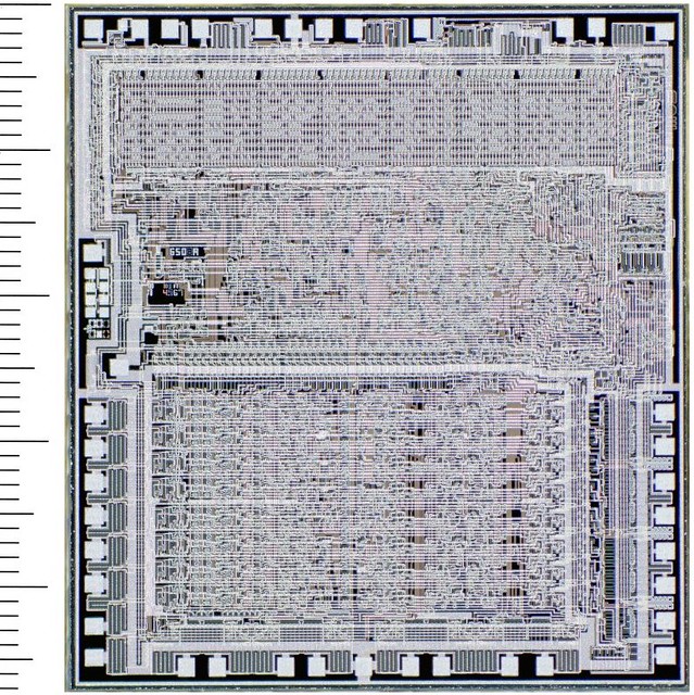
Photomicrograph © Antoine Bercovici (@Siliconinsid), reproduced with permission
Semiconductor Fabrication and the 6502
The 6502 was first delivered to customers in September 1975. This was one of a few iconic microprocessors of the late 1970s and early 1980s. To understand how big of an impact this chip had, all you have to do is look at its presence in many of the 8-bit systems of the era, sold by the millions:
- Apple II
- Atari 400 and Atari 800
- Atari VCS (6507)
- BBC Micro
- Commodore PET and VIC-20
- Commodore 64 (6510)
- Commodore 128 (8502)
- Nintendo Entertainment System (Ricoh 2A03)
The eventual ubiquitousness of the 6502-based personal computer was the end result of a long process that began thanks to Motorola for its pricing intransigence of the 6800 processor, and to Chuck Peddle and Bill Mensch for getting frustrated with Motorola. In March 1974, Motorola had announced the 6800, but did not reach production until November 1974, initially selling the chip for \$360 per processor in small quantities. Chuck Peddle had been giving marketing seminars to large customers in early 1974 — he’d smelled opportunity and tried to convince Motorola to pursue a lower-cost version for the industrial controls market, but they weren’t interested.[1 page 24-26] By August, Peddle had hatched a plan, leaving Motorola and setting off across the country to join MOS Technology, a scrappy little integrated circuit manufacturer located near Valley Forge, Pennsylvania. Mensch, one of the 6502 designers who went to MOS with Peddle, says this: “The environment was a small company where Mort Jaffe, John Paivinen, Don McLaughlin, the three founders, had created small teams of very capable calculator chip and system designers, a quick turn around mask shop and a high yielding large chip manufacturing team out of TI. So you go from Motorola with, relatively speaking, an unlimited budget for design and manufacturing, to an underfunded design team with very limited design tools for logic and transistor simulation. We had to manually/mentally simulate/check the logic and use very limited circuit simulation. In other words, it was really low budget. The datasheets and all documentation was done by the design team.”[2][3] Peddle persuaded Mensch and six other Motorola engineers — Harry Bawcom, Ray Hirt, Terry Holdt, Michael Janes, Wil Mathys, and Rod Orgill — to join him and a few others at MOS in designing and producing what became the MCS 6501/6502 chipset. “At MOS John Paivinen, Walt Eisenhower, and Don Payne, head of the mask shop, and mask designer Sydney Anne Holt completed the design and manufacturing team that created the high yielding NMOS depletion mode load process,” says Mensch. “The result was the MCS 6501/6502, 6530/6532 Ram, ROM Timer and IO combo and 6520/6522 PIA/VIA microprocessor family.”[3]
Some technical details of the 6502 are slightly fuzzy after so much time has passed — but I have chosen to focus on the 6502 because it is such a well-known processor, and at least some details are available. Semiconductor manufacturers are notoriously secretive, and it is hard to find detailed descriptions of how modern ICs are designed and manufactured. Whereas there are plenty of sources of information about the 6502.
(A word about the numbered notes: I don’t normally use such things, preferring instead a blogorrhific style of adding hyperlinks all over the place to point towards further information on various topics. But in this article, I have used notes to cite my sources a little more formally, for a few reasons. First, because there are inaccuracies about the 6502 floating about on the Internet, I’m trying to be a bit more careful. And since I’m not an expert in semiconductor manufacturing or economics, I feel like I have to point toward some specific accounts that back up my statements. Finally, a citation is a little more robust than a hyperlink in case an online publication becomes unavailable.)
EDN had a nice technical writeup of the 6502 in September 1975. BYTE magazine covered the 6502 in November 1975, with more of a focus on its instruction set than the physical aspects of the chip itself. Mind you, both these articles predated the use of the 6502 in any actual computer.
The manufacturing process for semiconductors is like printing newspapers. Sort of. Not really. Maybe more like the process for creating printed circuit boards. Well, at any rate, newspapers and printed circuit boards and semiconductors have these aspects in common:
- Production requires a big complicated manufacturing plant with many steps.
- Photolithography techniques are used to create many copies of a master original.
- The master original requires creating content and layout that fits in a defined area.
Except that the semiconductor industry has been expanding for decades without any sign of letting up, whereas the newspaper industry has been struggling to survive in the age of the Internet.
Semiconductor manufacturing occurs in a fabrication plant or “fab”. The raw, unpackaged product is called a die (plural = “dice” or “dies” or “die”), and the master original is called a photomask set or mask set. Engineers cram a bunch of tiny shapes onto the photomasks in the mask set; each of the photomasks defines a separate step in the photolithography process and is used to form the various features of individual circuit elements — usually transistors, sometimes resistors or capacitors — or the conducting paths that interconnect them, or the flat squarish regions called “bonding pads” which are used to connect to the pins of a packaged chip. Ultrapure, polished circular semiconductor wafers are used; most often these are made of silicon (Si), but sometimes they consist of other semiconductor crystals such as gallium arsenide (GaAs), gallium nitride (GaN), silicon carbide (SiC) or a hodgepodge of those elements somewhere towards the right side of the periodic table: AlGaAsPSnGeInSb. These wafers are sawn as thin slivers from a monocrystalline boule, basically a big shiny circular semiconductor salami, which is typically formed by pulling a seed crystal upwards, while rotating, from molten material, using the Czochralski process, which is very hard for us to pronounce correctly.
The wafers have a bunch of die arranged in an array covering most of the wafer’s surface; these are separated into the individual die, and go through a bunch of testing and packaging steps before they end up inside a package with conductive pins or balls, through which they can connect to a printed circuit board. The packaged semiconductor is an integrated circuit (IC) or “chip”. The percentage of die on a wafer that work correctly is called the device yield. Die size and yield are vital in the semiconductor industry: they both relate directly to the cost of manufacturing. If chip designers or process engineers can reduce the die area by half, then about twice as many die can be fit on a wafer for the same cost. If the yield can be raised from 50% to 100% then twice as many die can be produced for end use, for the same cost. Yield depends on numerous processing factors, and gets worse for large die ICs: each specific manufacturing process has a characteristic defect density (defects per unit area), so a larger die size raises the chance that a defect will be present on any given die and cause it to fail.
Think of defects as bullets that kill on contact. The figure below shows three simulated circular wafers with 40 defects in the same places, but with different die sizes. There are fewer of the larger die, and because each die presents a larger cross-sectional area which is prone to defects, the yield ends up being lower.

The steps of the photolithography process are performed under various harsh environmental conditions — 1000° C, high pressure or under vacuum, and sometimes with toxic gases such as silane or arsine that often react violently if exposed to the oxygen in air — and generally fall into one of the following categories:
- depositing atoms of some element onto the wafer
- coating the wafer with photoresist
- exposing the photoresist to light in a particular pattern (here’s where the photomasks come in)
- etching away material
- annealing — which is a heating/cooling process to allow atoms in the wafer to “relax” and lower crystal stress
- cleaning the wafer
And through the miracle of modern chemistry, we get a bunch of transistors and other things all connected together.
The term “process” in semiconductor manufacturing usually refers to the specific set of steps that are precisely controlled to form semiconductors with specific electrical characteristics and geometric tolerances. ICs are designed around a specific process with desired characteristics; the same process can be used to create many different devices. It is not a simple manner to migrate an IC design from one process to another — this is an important contributor to today’s supply chain woes.
Let’s look at that photomicrograph again:
Photomicrograph © Antoine Bercovici (@Siliconinsid), reproduced with permission
The original 6502 manufactured in 1975 contained 3510 transistors and 1018 depletion-load pullups, in a die that was 0.168 inches × 0.183 inches (≈ 4.27mm × 4.65mm), produced on a 3” silicon wafer.[4] The process used to create the 6502 was the N-channel Silicon Gate Depletion 5 Volt Process, aka the “019” process. Developed at MOS Technology by Terry Holdt, it required seven photomasks, and consisted of approximately 50 steps to produce these layers:[5][6]
- Diffusion
- Depletion implant
- Buried contact (joining N+ to poly)
- Polysilicon
- Pre-ohmic contacts
- Metal (aluminum)
- Passivation (silicon dioxide coating)
You can see these layers more closely in higher-resolution photomicrographs — also called “die shots” — of the 6502. Antoine Bercovici (@Siliconinsid) and John McMaster collaborated on a project to post 6502 die shots stitched together on McMaster’s website, where you can pan and zoom around. (If you look carefully, you can find the MOS logo and the initials of mask designers Harry Bawcom and Michael Janes.) I think the most interesting area is near the part number etched into the die:
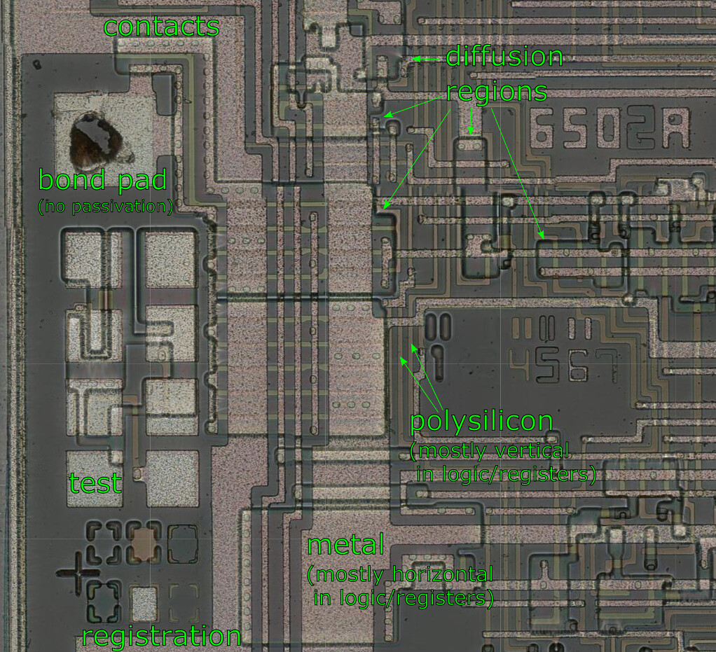
Photomicrographs © Antoine Bercovici (@Siliconinsid), stitched and hosted by John McMaster.
Annotations are mine. There is a small photo-stitching discontinuity between the top 1/3 and bottom 2/3 of this image.
The large squarish features are the bonding pads, and are connected to the pins of the 6502’s lead frame with bond wires that are attached at each end by ultrasonic welding, sometimes assisted by applying heat to the welding joint. (I got a chance to use a manual bond wiring machine in the summer of 1994. It was not easy to use, and frequently required several attempts to complete a proper connection, at least when I was the operator. I don’t remember much, aside from the frustration.)
The little cross and rectangles are registration marks, to align the masks and check line widths. The larger squares above them are test structures, which are not connected to any external pins, but can be checked for proper functioning during wafer probing.

Photomicrograph © Antoine Bercovici (@Siliconinsid), reproduced with permission.
This image is a composite of two photographs taken at the same 200× magnification: the 6502 die on the left, and a scale on the right with 10 microns per division (100 microns between major tickmarks).
The different layers have different visual characteristics — except for the depletion layer — in these images:
- the silicon substrate is an untextured gray
- the aluminum metal has a granular quality
- it has a pinkish tinge when it has been covered by the passivation layer (most of the die)
- when uncovered, as in the bonding pads and test pads, it is a more gray color
- the small green dots represent contacts between metal and silicon
- diffusion regions have a glassy look with discoloration around the edge
- polysilicon shows up as light brown, except when it crosses through a diffusion region, where it is greenish and forms a MOSFET gate — Tada! instant transistor! — controlling whether current can flow between the adjacent diffusion regions. (Ken Shirriff has some more detailed explanations with images for some features of the 6502.)
How many chips are on a wafer? It’s hard to find that information for the 6502, but Wikipedia does have a description of the Motorola 6800:
In the 1970s, semiconductors were fabricated on 3 inch (75 mm) diameter silicon wafers. Each wafer could produce 100 to 200 integrated circuit chips or dies. The technical literature would state the length and width of each chip in “mils” (0.001 inch). The current industry practice is to state the chip area. Processing wafers required multiple steps and flaws would appear at various locations on the wafer during each step. The larger the chip the more likely it would encounter a defect. The percentage of working chips, or yield, declined steeply for chips larger than 160 mils (4 mm) on a side.
The target size for the 6800 was 180 mils (4.6 mm) on each side but the final size was 212 mils (5.4 mm) with an area of 29.0 mm². At 180 mils, a 3-inch (76 mm) wafer will hold about 190 chips, 212 mils reduces that to 140 chips. At this size the yield may be 20% or 28 chips per wafer. The Motorola 1975 annual report highlights the new MC6800 microprocessor but has several paragraphs on the “MOS yield problems.” The yield problem was solved with a design revision started in 1975 to use depletion mode in the M6800 family devices. The 6800 die size was reduced to 160 mils (4 mm) per side with an area of 16.5 mm². This also allowed faster clock speeds, the MC68A00 would operate at 1.5 MHz and the MC68B00 at 2.0 MHz. The new parts were available in July 1976.
The MOS Technology team seized the opportunity and beat Motorola to production with a depletion-load NMOS process (“regular” enhancement-mode N-channel MOSFETs acted as pull-down switches; depletion-mode N-channel MOSFETs were used as a load, with their gate and source tied together to act as a current source) in the 6502, which allowed the design team to achieve higher performance in a smaller die size.


Left: NAND gate with saturated enhancement-load NMOS. Right: NAND gate with depletion-load NMOS. In both cases, T1 acts as a current source, so that the output Y is low only if both A and B are high, but the depletion-mode version of T1 maintains strong current-source behavior at a higher output voltage than the enhancement-mode version, achieving faster rise times for the same static power dissipation. (Images courtesy of Wikipedia)
For the most part, design of the 6502 was paper-and-pencil, with some computer-assisted aspects of layout. Peddle was project leader, and focused on the business aspects; he also worked on the instruction set architecture — basically the abstract programmer’s model of how the chip worked, including the various opcodes — with Orgill and Mathys.[7]
To reduce this to a working circuit design, the 6502 team had to come up with a digital design of instruction decoders, arithmetic/logic unit (ALU), registers and data paths (high-level register-centric design) that could be implemented using individual gates made out of the NMOS transistors and depletion loads (low-level circuit design). Peddle, Orgill, Mathys, and Mensch worked out the register structure and other sections of the high-level design,[1 page 28][8] with Mathys translating a sequence of data transfers for each instruction into state diagrams and logic equations.[8] Mensch and Orgill completed the translation of the register-centric design from logic equations into a circuit schematic (technically known as the “650X-C Microprocessor Logic Diagram”[9]) of the NMOS transistors and depletion loads, annotated with dimensions, while Wil Mathys worked on verifying the logic.[10]
Mensch describes Orgill and himself as “semiconductor engineers”, responsible for reducing logic equations to transistor-level implementation in an IC to ensure that it meets speed, size, interface compatibility, and power specifications.[11] Orgill’s specialization was on the high-level architecture, contributing to the ISA, with “a focus on logic design and minimization”,[11] whereas Mensch had a predilection for low-level details. Mensch determined the design rules, ran circuit simulations on portions of the chip — limited to around 100 components at a time with the computation facilities available to MOS Technology in 1975 — and designed in the two-phase clock generator that would become the distinguishing factor between the 6501 and the 6502.[11][12 page 19] (The 6501 and 6502 shared all masks except for the metal layer, which had two slightly different versions: the 6501 left the two-phase clock generator disconnected so that it was pin-compatible with the Motorola 6800, whereas the 6502 connected the clock generator circuitry, breaking pin-compatibility. In 1976, MOS Technology agreed to cease production of the 6501 as a condition of a legal settlement with Motorola.[13])
Orgill and Mensch drew the schematic on mylar, using pencils with plastic lead[14] which could be erased. I found a book that described drafting on mylar this way:[15]
Drawing on mylar for the first time can be a scary experience — both for the novice designer and the company. The surface of mylar drafting film holds drawing lead much more loosely than the fibers in paper. If you were to draw on mylar with a regular graphite “lead” pencil, the disastrous results would be like drawing on a sheet of frosted glass with a charcoal briquette. You could form the lines, but they wouldn’t be very durable against smudges.
To compensate for this lack of adhesion, special plastic lead was developed specifically for use on mylar drafting film. Instead of being made from graphite, this “lead” is made of a soft waxy plastic compound. It comes in varying degrees of hardness just like regular drafting pencils. The softest designation is E0, and they progress in hardness with E1, E2, E3, etc.
Here is one section of the schematic, showing a section of the ALU; the dashed lines each surround one bit of the ALU.[16]

Photo of a portion of the Hanson copy of the 650X-C Microprocessor Logic Diagram, taken by Jason Scott.[17]
The annotations here include two types. The letters A-Z and AA-JJ, according to Mensch, denoted individual transistors for the purposes of checking correctness in the layout.[16] The numbers indicate transistor dimensions, in mils (thousandths of an inch), and are listed in two forms:[14]
- A single number denotes NMOS gate widths, with a standard gate length of 0.35, the minimum used in this design
- A pair of numbers W/L with a dividing line denotes gate width and length — current in the transistor is proportional to W/L, which determines how small and how fast each transistor is.
The transistor at the output of a gate is a depletion-mode pull-up, with the others as enhancement-mode transistor inputs[14] — so, for example, the NOR gate with transistors AA and Y as inputs had gate widths of 0.7 mil and length of 0.35 mil, and a depletion-mode pull-up of 0.3 mil width and 0.8 mil length. (In theory, someone could double-check this against Antoine Bercovici’s die photos of the 6502 rev A, by locating individual transistors and trying to find the corresponding transistors on the logic diagram… I have not, and leave this as an exercise for the industrious reader.)
The minimum gate length of 0.35 mil implies a technology node of 0.35 mil ≈ 8.9 micron for the 6502.
There are a few other interesting things visible from the schematic — the use of dynamic logic, for example. Anytime you see clock signals (ϕ1 and ϕ2 are the two-phase clock signals on the 6502) doing weird stuff, where some logic gate doesn’t have any driving input part of the time, you know you’ve got dynamic logic going on. (Wikipedia says “Dynamic logic circuits are usually faster than static counterparts, and require less surface area, but are more difficult to design.”) What caught my eye was the “T” and “B” on these AND gate inputs shown below:

Photo of a portion of the Hanson copy of the 650X-C Microprocessor Logic Diagram, taken by Jason Scott.[17]
I asked Mensch about this; he said they stood for “top” and “bottom”, specifically referring to the implementation of an AND or NAND gate in depletion-mode NMOS.[16] Here’s a transistor-level implementation of that pair of AND gates followed by a NOR gate:

Transistors Q1 (top) and Q2 (bottom) would correspond to one T/B pair of AND-gate inputs, and Q3 (top) and Q4 (bottom) the other. This matters because switching speed is different for the top and bottom MOSFETs — the top ones have drain-to-gate capacitance slowing down the switching (the Miller effect), whereas the bottom ones see a low-impedance load from the top transistors, forming a cascode configuration. As to why that is critical here, I’m out of my element — Mensch says the bottom transistor should be the first transistor to change state, and the last signal to change should be the top transistor[18] — but the point here is that digital logic design is not just a nice little abstraction layer with ones and zeros based on simple, identical, combinational logic and flip-flops. A lot of work went into choosing transistor sizes to get the 6502 to work fast under die size constraints.
The schematic also served as a rough layout known as a floorplan showing high-level placement, with the various gates arranged on the schematic roughly where Mensch thought they should go on the chip.[19] Bawcom, Holt, and Janes were mask designers for the 6502 chipset, taking the circuit design and placement and implementing them as individual transistors or resistors, made out of rectangular features sketched on various layers of Stabilene mylar film.

Image from Hoboken Historical Museum
The mask designers did not draw these features directly by hand — when I first started reading historical accounts of the 6502 for this article, I had a mental image of them sketching transistors on Stabilene one by one, fitting together like a puzzle until the last pieces were drawn in… and dammit, there’s only enough room for seven flip-flops, not eight, so they’d have to start over and try again. But that’s not how it worked. Instead, the design was based on “cells”, small reusable pieces of the design that could be planned separately and then fit into place in the layout, like Escher tesselations all coming together, or some kind of sadistic furniture floor plan where the room is full of tables and chairs and sofas with no space between them. Harry Bawcom, who previously worked on bipolar TTL layout at Motorola and was brought in to finish the 6800 microprocessor layout,[20] described cells this way:[21]
Cell design started with little stickies of transistors underneath clear mylar and you did the first pass with a grease pencil and a lot of iteration. That was a Bipolar technique that the MOS folks didn’t use. Probably why I was five times faster. By the time I picked up a pencil I knew where I was going.
According to Mensch, these physical representations of cells used in drafting were also called “paper dolls”, a term that shows up every now and then in accounts of that era. Joel Karp, the first MOS chip designer at Intel, also used this term describing the rather painstaking layout process for the Intel 1102 and 1103 1024-bit DRAM ICs.[22] Another account, from New York’s Museum of Modern Art, described a Texas Instruments logic chip layout from around 1976:[23]
At the time this plot was hand drafted, it was still possible to verify the design of individual components visually. To repeat a circuit element multiple times, an engineer would trace the initial drawing of the component, photocopy it onto mylar, then cut and glue it onto the diagram. The collage technique is referred to as “paper-doll layout.” Intended for use in a military computer, this particular chip was designed to sense low-level memory signals, amplify the signals to a specific size, and then store them in a memory cell for later recall.
But the early microprocessor designs at Motorola and MOS Technology were just starting to emerge from the manual-only world. Here the computer-assisted aspects came into play: for the 6502, someone at MOS captured each cell on the Stabilene film using a Calma GDS workstation and digitizer.[24][12 page 12] (Bawcom refers to this person as the “Calma operator” but says he “did not witness this process at MOS Technology.”[21]) Where possible, the Calma workstation was used to replicate cells that could be repeated in the design.[21]

Digitizer table for capturing IC design at MOS Technology, titled "DATA INPUT FOR AUTOMATIC MASK PREPARATION" on a MOS Technology brochure from 1970, courtesy of Diana Hughes and Team6502.org.
The digitizer was a drafting table with a precision position sensor that could record x-y coordinates of any position on the table. The workstation was a Data General Nova minicomputer[25] with 5 megabyte hard drive and 16K RAM. The minicomputers at that time were created mostly out of standard logic chips (like the 7400 series) in DIP packages — each typically containing an array of 2-8 components like gates, registers, multiplexers, etc. — soldered onto circuit boards to make a processor and other associated sections. A cabinet-sized computer, rather than a room-sized mainframe. (If you haven’t read Tracy Kidder’s Soul of a New Machine, make a note to do so: it chronicles the design of the Data General Eclipse, the successor to the Nova.) The Calma GDS stored the layout design as polygons and could be used to draw the layout on a plotter, or to cut a photomask drawing out of a red film called Rubylith, also using the plotter, but with a precision blade used in place of a plotter pen.[12 page 12][26] Then the unwanted sections of Rubylith would be removed very carefully by hand during what MOS Technology engineers called a “peeling party”, according to Albert Charpentier.[26]

After a lot of very careful checking and revision, the set of Rubylith photomask drawings — shown in this picture from the August 25, 1975 edition of EE Times — were photographically reduced to a set of master glass reticles, one per mask, at 10 times actual size.[24] Each 10× reticle was used to reduce the design further, producing a 1:1 mask using a machine called a reduction stepper, which precisely locates multiple copies covering most of the 3-inch[24][27] wafer. In early production, contact or proximity masks were used,[12][28][29] but once MOS had been able to upgrade to four-inch wafers,[29] a Perkin-Elmer Micralign projection mask aligner[27][1] was used to scan the 1:1 mask bit by bit, using a clever symmetrical optical system, for lithography steps.[30]
The Micralign projection aligner was one of several reasons the 6502 team was able to succeed, by improving yields. (Remember: die size and yield are vital!) Motorola’s NMOS process yields were poor[31][32], giving them cost disadvantages. Mensch says that Ed Armstrong, Motorola’s head of process engineering at the time, grew out his beard, waiting to shave it until they were able to get 10 good die on a wafer.[12][19][10] The MOS team was able to get much higher yield than Motorola, in part by using a projection mask system: previous-generation lithography systems used contact masks, which touched the wafers and had limited durability. Motorola had used contact masks for the 6800.[1 page 22] From Perkin-Elmer’s Micralign brochure:[33]
Historically, the manufacture of integrated circuits involved placing the photomask directly in contact with the wafer during the exposure process. Repeated just a few times, this contact soon degraded the mask surface and the photoresist layer. Each defect that resulted was then propagated through the replication cycle. Consequently, masks were considered expendable, to be used between five and fifteen times and then discarded.
These problems led to several attempts at prolonging mask life. One was to make the photomask from harder materials that were more resistant to abrasion. Another was to reduce abrasion by reducing or even eliminating the contact force. These efforts did improve mask life to a limited extent, but neither was as effective as optically projecting the photomask image onto the wafer.
A second reason for the 6502’s higher yield was something MOS Technology referred to as “spot-knocking”[12 page 18], essentially a retouching of point defects in the masks.
The third reason for higher yields was through Mensch’s design rules — constraints on transistor size and feature spacing — which were conservative and much more tolerant of process variations,[19] a technique which he had learned on his own through experiences at Motorola, along with some lessons about what was and what wasn’t possible to achieve at the company.
Mensch’s first year at Motorola in 1971 was a rotation through four different departments: Applications, Circuit Design, Process Design, and Marketing.[34] At the Marketing department, his supervisor Dick Galloway asked him to put a quote together for IBM for memory chips over a seven year period, with pricing decreasing over time — a fairly complicated document, with lots of numbers that had to be typed accurately. So he decided rather than having a secretary type it up and go through the trouble of finding and correcting errors, he would write a FORTRAN program on the Motorola mainframe computer to take in parameters, plug in the numbers into some formulas, and print out the quote on a terminal with a thermal printer, which he then copied onto better paper. The Marketing staff asked him how he did it, and when he told them, Galloway said “Bill, we want you to work in the Design Group.” “Why is that?” “None of their chips work. We want you to work there. I think if you work there, the chips will work again.”[12][19]
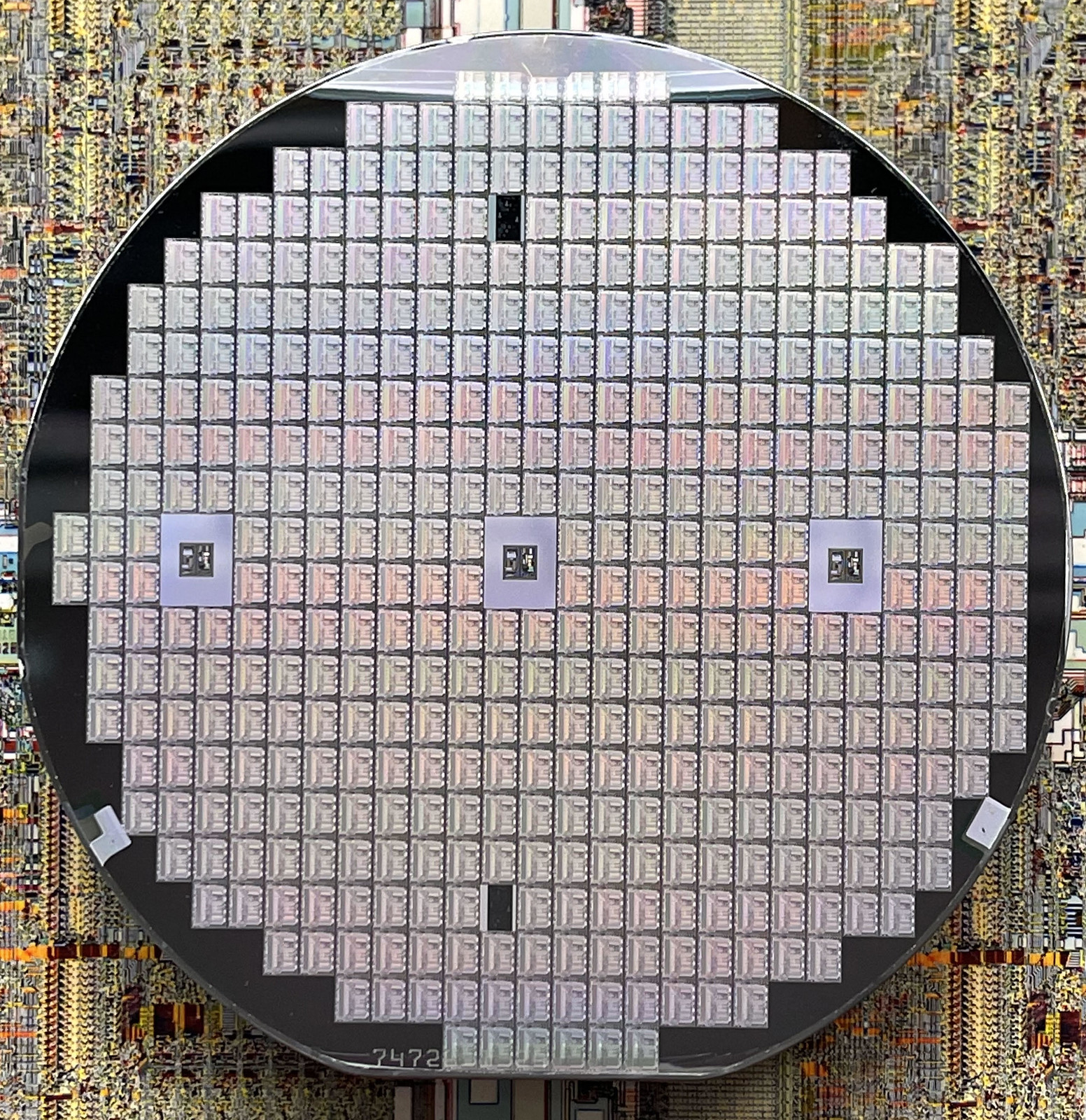
As the new, inexperienced engineer in the IC design group, Bill Mensch’s introduction involved a lot of what the other engineers would call grunt work. Some of these efforts were to work on Motorola’s standard cell library in various MOS processes, and the process control monitor for memory and microcontroller designs.[24][12] The process control monitor (PCM) is a special set of test structures used to measure the parameters of basic circuit elements such as transistors, resistors, capacitors, and inverters — not only to make sure the manufacturing process is working as expected and check for statistical variation, but also to characterize these elements for simulation purposes. Nowadays it is typical to put those test structures in the scribe lines between ICs, since they can be so small, but in earlier IC designs the PCM is located in a few places on the wafer in place of the product, usually forming a plus-sign pattern of five PCMs. Early 6502 wafers from MOS Technology are — in 2022 at least — apparently nowhere to be found, but occasionally some later MOS wafers show up on eBay, and I did find a creator of “digital art”, Steve Emery at ChipScapes, who had a 4-inch Rockwell R6502 wafer, apparently from the mid 1980s (Synertek and Rockwell were both licensed by MOS Technology as a second-source for the 6502) on which you can see the PCMs. He was kind enough to take some photomicrographs of them for me:
Rockwell R6502 photograph © Steve Emery, reproduced with permission.
Ray Hirt designed the PCMs for the MOS 6502[24]; the Rockwell PCMs shown here are almost certainly not the ones Hirt designed in 1974-1975, but the overall concept is the same. The Rockwell R6502 has two different types, three of one type in the middle rows of the wafer, and two of another type in the top and bottom.

Rockwell R6502 photograph © Steve Emery, reproduced with permission.
The ones on the top and bottom look like an image resolution test on the various layers; there are no electrical connections:

Rockwell R6502 photograph © Steve Emery, reproduced with permission.
The three others have a bunch of circuit pads connected to various test elements:

Rockwell R6502 photograph © Steve Emery, reproduced with permission.
The PCMs that Mensch and Hirt designed included transistors of various dimensions, digital inverters, and ring oscillators. The inverter could be used to measure the input-output transfer function; the ring oscillator for measuring intrinsic time delays. The transistors typically included a minimum-size transistor (0.4 mil × 0.4 mil ≈ 10 μm × 10 μm in the early 1970s), and others with different widths and lengths, so that the parameters of the transistors could be characterized as a function of geometry.[2] In a 2014 interview, Mensch describes the PCMs during his early days at Motorola this way:[12]
We had to make some changes to model because of things I found. And I found that narrow transistors had a higher voltage threshold than a short one, and these are things that the memory product guys didn’t use. And so they had to change their design because of what I found on the process control monitor. I put very narrow transistors, very wide transistors, very large transistors, and very short transistors, so I knew the characteristics and what the actual sizing might have an effect on.
When I spoke with him in March, he described his experience a bit more candidly. As a young engineer at Motorola trying to learn the best way to design ICs, Mensch wanted to know what numbers to use for a transistor simulation model, so he asked around, and each of the design engineers had different numbers they used in their calculations; a typical exchange went like this:[2]
Mensch: Why are you using those numbers?
Engineer: Well, I just think it’s the right number.
Mensch: Yeah, but… but… who’s… who’s giving out the numbers? What temperature are you simulating it at?
Engineer: Well… at room temperature.
Mensch: Well, why room temperature?
Engineer: Well, that’s what we take the data on.
Mensch: Yeah, but you know it’s gonna run at 125°C, right? And minus 55, we need to get them to work that way.
Engineer: Yeah, but… whatever.
Mensch’s voltage threshold discovery — that gate threshold voltage on the same process varied with transistor geometry, and a good model would have to take this into account — was not immediately well-received; at first, engineers from the memory group didn’t believe him. He ended up sending around an inter-office memo to call a meeting (“MEETING TO PICK BILL’S SIMULATION NUMBERS”) and got everybody to attend by the happy accident of including Jack Haenichen on the cc: list of the memo. Haenichen was Motorola’s youngest vice-president, first elected in 1969 to become Vice President and Director of Operations, Services and Engineering in Motorola’s Semiconductor Products Division, at the age of 34; in early 1971 he was renamed to Director of Operations for MOS.[35][36][37] Haenichen had taken an interest in Mensch’s progress during his rotation in the Marketing department, and asked to be kept informed how things were going. As Mensch described it: “So this interoffice memo, everybody would see, ‘Hey, Jack’s on this list! Oh, we gotta show up.’ I never realized why all these people showed up at my meeting.” He eventually chose simulation parameters that were the worst case of all the other numbers.[2]
Over the next few years, an opportunity had begun to arise. Mensch was no longer a green engineer; by 1974, he had designed the 6820 Peripheral Interface Adapter, and he and Rod Orgill had worked together on design teams for two microprocessors at Motorola — the 5065, a custom microprocessor for Olivetti, and the Motorola 6800.[3] Mensch also had designed the PCM for the 6800, and put in test structures not only for the enhancement-load process of the 6800, but also for a depletion-load process, all ready to help prove out the superiority of the concept, just by making a slight change in the masks and the processing steps.[12] Meanwhile, Chuck Peddle had joined Motorola, and in 1974 was traveling the country giving seminars on the 6800 for prospective customers, who were very interested, but not at the price Motorola was offering. Peddle wanted to pursue a lower-cost version of the 6800.[1] Motorola had advantages in financial resources; the company’s 1972 Annual Report stated proudly that its revenues exceeded a billion dollars for the first time, and “Metal-oxide-semiconductor (MOS) integrated circuit sales for Motorola during ’72 grew at a faster rate than the world industry, whose growth was an estimated 60-70%.”[38] In 1973’s Annual Report, it stated \$1.437 billion in revenue, with the company’s Semiconductor Products Division reporting revenue “up more than 45% over the previous year”, and expressed an optimistic view of the microprocessor market:[39]
The burgeoning microprocessor market is presenting the industry with a radical opportunity to engineer into electronic systems significant benefits not previously possible. The true extent to which microprocessors will be adopted is not yet apparent, even though the current picture indicates a possibly phenomenal market whose growth rate could eclipse that of today’s fastest growing semiconductor categories. Motorola has a major commitment to the microprocessor market, and we intend to secure a significant share. Development in this area has reached an advanced stage.
Motorola had already been in the electronics business for decades — starting with car radios in 1930 and getting into the semiconductor market with mass-production of germanium power transistors in 1955 — with a well-established sales and distribution network. It had the tools and staff to design and manufacture cutting-edge microprocessors.
So why was the low-cost 8-bit microprocessor a project at MOS Technology instead of Motorola?
The Elephant and the Hare
I have struggled to understand: Why not at Motorola? Motorola had all these resources, and an opportunity to follow up on the 6800, but at first glance appears to have squandered the opportunity.
Motorola and MOS Technology were two very different companies. In Motorola’s case, being a large company gave it significant long-term advantages, in the form of product diversity — Motorola was nearly a self-contained “supermarket” for the circuit designer, with discrete, analog, and digital ICs, so it benefited from many market trends in electronics — and inertia. Its size allowed Motorola some freedom to “coast”, when necessary, on its past successes. MOS Technology was small and agile, and had to survive by being competitive in a few specific areas like MOSFET-based IC design and manufacturing technology. A business failure of a few million dollars would have been a minor setback for Motorola, but a mortal wound for MOS.
A 1970 ad campaign describes “Motorola’s Ponderous Pachyderm Syndrome”,[40] something that seems like incredibly poor marketing:

Haenichen described in an interview:[41]
Motorola, at the time, was called the “Ponderous Pachyderm” by the industry people. In other words, we maybe were not the “latest and greatest” but when we started making something, we wiped everybody out, because we just made them by the billions — that was our reputation, slow moving but good.
Yeah, um… okay. I get the idea. Take a little longer and become a dominant player in the industry… sure. But a “ponderous pachyderm” as high-tech corporate metaphor? Not exactly the most inspiring.
And yet, if we fast-forward to the 1980s and 1990s: Motorola did find success in its microprocessor offerings, reaching its zenith a few years after the 6800 and its follow-up, the 6801 — in the form of the 68000 series, which were produced roughly from 1979 - 1994 and used in many systems, notably the Apple Macintosh. And later 6800-series ICs like the 68HC11 took a prominent position in the microcontroller market.
Even by early 1980, the 6800 and 6809 achieved market success. While looking for historical pricing information in Byte Magazine’s January 1980 issue, I came across several ads for third-party systems and software tools for the 6800 and 6809. The chip distributor ads in the back of the magazine listed various microprocessors, almost all in the \$10 - \$20 range, including the Zilog Z80, the 6502, the 6800, RCA’s CD1802, and Intel’s 8080. Motorola had been able to lower the cost of the 6800.
But 1974 was a different story. With a major economic recession looming, Motorola’s Semiconductor Products division turned more risk-averse, and focused on getting the 6800 out the door successfully. Mensch, who had worked on the 6800’s process control monitor, and snuck in a depletion-load version in addition to the normal enhancement-load PCM, was pushing to have one wafer ion-implanted to try out the depletion-load process. When he talked to Armstrong (head of process engineering) he was finally told why they wouldn’t let him investigate depletion-mode: “We were afraid you wouldn’t complete the designs with enhancement mode.”[19]
Tom Bennett, who led the chip design of the 6800, described relying on depletion loads as “a little risky”:[31]
We did the ion-implant only of the substrate. There was an extra one or two process steps to do the depletion load. And it was determined that, you know, that might be a little risky. That’s why we went to all these other, you know, hardware extremes to get around that. And so we compensated for it with design.
Given the process problems Motorola was having with just getting enhancement mode NMOS to work, perhaps this was the right decision for Motorola after all.
Internal politics and friction also hampered the 6800 project.[42] The sense I get, in talking to Bill Mensch and reading other accounts of the 6502 and 6800, was that at Motorola, getting things done depended on being on good terms with other staff and with managers — the old adage, it’s not what you know, it’s who you know. Bill Lattin, a member of the Motorola design team interviewed by the Computer History Museum in 2008, described this environment’s effect on the 6800 this way:[43]
Well, the amazing thing is that it succeeded as well as it did. Having gone to Intel and seeing a very — a company that does a very structured strategic plan every year, and knows where to focus the resources, Motorola was a bottoms-up. A strength of an idea would get sold, and or Doug Powell would get it and he would push it. And then Tom would get it, and convince everybody, you know, we want to work on that. And it was, you know, having now been in management, and looking back I kind of say, “What could have happened here with 6800 had there been strategic direction from the whole company, you know, moving down this way?” And so it was a phenomenal success. I’m privileged to have worked with really bright guys pulling it off, and against chaos that was put in everybody’s way.
The 6800 team succeeded in getting management buy-in; Peddle and Mensch did not with their low-cost microprocessor. But Peddle joined the 6800 team fairly late in the project, and Mensch was a junior engineer learning the hard way that technical merit was not enough.
Aside from the recessionary climate and internal politics, there is one more significant reason that dampened Motorola’s eagerness towards pursuing microprocessors. Being a large, diversified company sometimes presented a conflict of interest between Motorola’s different semiconductor groups. Even the 6800 team faced this: each market opportunity for the company to sell an integrated microprocessor like the 6800 would compete against circuit-board-level processors designed with less-integrated logic chips. Within Motorola, that would mean less business selling standard logic chips, and among Motorola’s customers, it might put some of the minicomputer companies’ designs at risk.[44] From the Computer History Museum’s 2008 interview:[43]
Bennett: And interesting. The only one that really asked some questions which I thought were important was Bob Galvin. And his comment was when he looked at it he says, “You understand that you’re putting our customer’s chip — or system — on one of these little boards?” He said, “What’s that gonna do to my other products?” But that’s where it was at that point in time. The other thing…
Ekiss: Yeah, HP really recognized that, because I had called on them as a customer, and they quizzed me up and down about the implications for the semiconductor company to be able to make products like this. Because we were now right on their turf.
Laws: We did the recording of the 8008 oral history several months ago, and listening to the tremendous battles that went on in Intel between the memory people who were terrified that processor people were going to be treading on their [customer’s] turf and taking away their business. So it was not unique to Motorola.
There’s a gap in the historical record here: it would be nice to find a well-reasoned explanation from Motorola’s management why they told Peddle to stop working on a low-cost microprocessor.[45] But I will hazard a guess: just consider that in 1974, Motorola was still trying to bring the 6800 to production so they could start selling it to make some money back on their investment — John Ekiss related that they had been relying on income from large customers like National Cash Register, who’d been buying ROMs, to fund new engineering efforts[43] — and here’s this guy Peddle who’s been at Motorola for less than a year, squawking about how they need to sell a lower-cost processor, which would potentially compete with the 6800 that hadn’t even been released yet, and which would earn Motorola less profit per processor sold. Oh, and yes, there’s a recession going on. So please, Chuck, stop it and help us sell the 6800.
Sometime around early 1974, management announced that the microprocessor group would be moving from Mesa, Arizona to Austin, Texas — an unpopular decision — and at about that point Peddle proposed jumping ship.[1][12][43]
In one presentation, Mensch alludes to Star Wars, describing the eight departing Motorolans as “Rebels” leaving the Motorola “Empire”,[24] going to MOS Technology instead, in order to make their vision into reality. In some ways it is not surprising that they succeeded. Working with fewer resources and fewer people, the team had to be creative to make things work, but fewer people can also be an asset. In The Mythical Man-Month, Rodney Brooks talks about the concept of “conceptual integrity”, of having a unified design: “I will contend that conceptual integrity is the most important consideration in system design. It is better to have a system omit certain anomalous features and improvements, but to reflect one set of design ideas.”
Mensch related how Stephen Diamond asked him about the oscillator section of the 6502:[10]
And he says, “Bill, didn’t you have trouble with that?”
I go, “No, why, why do you ask? It was just, you know, you just know what the edges needed, so that the feedback from like the X register from the output to the input when you’re loading a new value, you want to not lose what’s in there while, you know, because you don’t want to feed back the output from it or you won’t load the new value right,” and I said, “so that we all knew what the timing was.”
But he says, “Well, we had to struggle with that and we had all kinds of—“
I said, “Oh, I think I know why. How many engineers did you have on it?”
“Oh, I don’t know, maybe 20.”
I go, “That’s the problem. We didn’t have that many engineers, so… ours worked.”
Mensch describes how leaving Motorola and getting to MOS allowed him and Rod Orgill to figure out how to design what they felt was the right microprocessor:[19]
Big companies sometimes manage the passion out of the engineers with broken promises and disrespect coming from management not knowing the effort needed for pioneering effort. At MOS with the small team we created and kept the passion to do the best humanly done. Since this was Rod’s and my third (6501) and fourth (6502) microprocessor designs following the Olivetti 5065 CPU and 6800, we knew what we had to do to make a processor to change the world of processing at the microprocessor level.
And unlike at Motorola, at MOS Technology there was no handicap in working on a low-cost state-of-the-art microprocessor, no other design groups or customers to worry about avoiding a conflict of interest.
From the first day the “Rebels” were on the payroll at MOS in Pennsylvania — August 19, 1974, freed from the Ponderous Pachyderm, and motivated to succeed — to bringing MCS 6502 chips into production, ready for sale, it would take just over a year.[12]
The 6502 was aimed to compete in price against the Intel 4040 in the microprocessor-based control systems market[46], but blew it away in technical specs: the 4040 was a 4-bit processor with a slower maximum clock frequency and required a 15V supply.
By summer of 1975, MOS Technology was gearing up for an introduction in September at WESCON 75 in San Francisco, and took out ads focused on the 6501:[47]

Ad courtesy of Wikipedia.
Here the story takes one of those legendary turns. Steve Wozniak had been designing the Apple I around the Motorola 6800, but he sees the MOS Technology ad, realizes he can get a better price (even better than a Motorola discount he can take advantage of as a Hewlett-Packard employee[48]), goes to WESCON, and buys a couple of chips from Peddle, who’s selling them in a jar from a suite in a nearby hotel because WESCON won’t let them sell product at the convention[49][10]. The 6502 is soon in the Apple I design. Only two hundred Apple I computers were manufactured in 1976, but by that time, Wozniak is already thinking about the Apple II, introduced in 1977, which will quickly take off like a rocket, starting the use of the 6502 in the personal computer industry with a bang.
The 1970s Pocket Calculator Crisis
But before Steve Wozniak and Steve Jobs incorporated as Apple Computer Inc., to bring Woz’s Apple II design to fruition, Wozniak was still an employee of Hewlett-Packard working on electronic calculators. Computers? No, calculators. (This is such a “Video Killed the Radio Star” moment in history.)
MOS Technology was still looking for customers. In September 1976, it was purchased by Commodore, a calculator manufacturer, in a move that, to me, appears to be one of financial desperation… but it set the combined company on an arc that lasted the next 18 years as it crossed into personal computers. The magazine New Scientist chronicled the tone of the times in two articles, the first in November 1975 (“Coming of Age in the Calculator Business”):[59]
… The LSI revolution started by specialist semiconductor suppliers like General Microsystems Inc along the 30 mile strip between San Francisco and San Jose (known nowadays as Silicon Gulch) effectively wiped out the cheap labour advantage of South-East Asia in a single stroke — and ensured that the market for pocket-sized calculators henceforth would be dominated overwhelmingly by US firms.
…
By 1971, Bowmar had successfully married a compact LSI chip to a small light-emitting diode (LED) display to provide what was to be the first truly compact, hand-held pocket-sized calculator using a chip developed by Texas Instruments. Incredibly, Bowmar was not interested in marketing the pocket calculator itself, and tried instead to sell the idea in turn to most of the leading manufacturers of electro-mechanical calculating machines. Commodore was one of the two firms that agreed to market the pocket calculator for them; the other was a home entertainment supplier called Craig.
So rapid was the take-off in the pocket calculator market that, by the following year, Bowmar was struggling to get back into the business. Another original component supplier, American Microsystems, also moved into calculator manufacture in 1972 under the trade name Unicom. This “vertical integration”, from the bottom up, then became the fashion. The world’s largest supplier of semiconductor components, Texas Instruments, started manufacturing calculators late in 1972, and was joined by National Semiconductor in 1973.
While the major semiconductor suppliers were attracted by the large profit margins on finished calculators, the leading calculator assembly houses grew anxious about the supply of components and several consequently began to integrate the business downwards. However, the more sensible stopped short of actually manufacturing chips, but designed their own integrated circuits and then farmed them out to other semiconductor suppliers to manufacture for them.
Though prices were still relatively high (the cheapest four-function machine still cost more than £30 in 1973), the pocket calculator quickly caught the public’s imagination. Sales rocketed, and prices crashed accordingly. Between 1968 and 1972, five of the original 18 firms involved in pioneering electronic calculators had dropped out, but 35 new names had joined the ranks. Since then, many other big names have fallen by the wayside, including Anita, SCM/Marchant, Rapidata, Summit, Seiko and Sony. Even Bowmar ultimately had to file for protection under “Chapter XI” of the US bankruptcy law. Unicom was submerged into Rockwell and Remington Rand departed from the field.
What happened to the profits?
This year the big vertically integrated calculator firms have seen their profits vanish, and some of the calculator assembly houses are now in really deep trouble. Even Commodore is struggling to survive. Two weeks ago the firm reported its end of year results, which showed a \$4.3 million loss on sales which were up 12 per cent over the year to \$55.9 million. Commodore is now pinning most of its hopes on the European market, which is nowhere near as stagnant as the American market has been lately.
Only a handful of calculator firms look like surviving the present recession and the names that British retailers quote with confidence include Texas Instruments, Hewlett-Packard, Commodore (CBM), Litronix and Sinclair. Vertical integration in itself is no longer seen as the best way of ensuring survival. Certainly firms like Texas Instruments, who make practically all the components that go into their calculators themselves, will continue to dominate the market — not by virtue of their vertical integration but really because of their overall financial strength. But given a replacement market of 50 million units per year, the industry is obviously settling down to an era of maturity, which will be dominated by one or two really large suppliers and supported by a number of smaller companies specialising in more innovative designs. The prices of pocket calculators are not likely to fall appreciably, but the user will continue to get increasing calculating power for his money.

Wow! This article was quite prescient, and seems to have got almost everything right, except for that bit about “The prices of pocket calculators are not likely to fall appreciably” — only a year later, Texas Instruments introduced the TI-30 in June 1976 for a \$24.95 suggested retail price. (TI achieved this price point by designing it around a single TI chip, the TMC0981.) The rest, about the consolidation of the industry and anxiety of calculator manufacturers as IC manufacturers got into the calculator business, was right on the money.
What I have not yet mentioned was that MOS Technology was started in 1969 by Allen-Bradley as a means to second-source TI’s calculator chips. Up until the 6502, the bulk of its business was in the calculator chip industry. With TI becoming a dominant force in the calculator industry, as its volumes surged and prices fell, MOS Technology was in trouble. Commodore was also in trouble, and at the very least saw a conflict of interest with TI (namely buying second-sourced TI chips when TI was a competitor for finished calculators) which it could solve by purchasing MOS Technology. New Scientist covered this in a brief filler article in its September 9, 1976 issue titled “Calculator manufacturer integrates downwards”:[60]

You will note that there is no mention whatsoever of the 6502; it is only hinted at: (emphasis is mine, along with bracketed annotations)
Commodore, the Canadian owned American based calculator manufacturer which markets under the name CBM in Britain, has announced its intention of entering integrated circuit component manufacture with a recent take-over. Unlike several of its competitors (such as Rockwell, National, and Texas Instruments) who are primarily microcircuit manufacturers but who have also integrated vertically upwards into end-products like calculators, Commodore is integrating downwards in order to protect its supply of components.
Commodore, quoted at \$60 million on the New York Stock Exchange, has acquired 100 per cent of the equity of MOS Technology Inc. of Pennsylvania in exchange for a 9.4 per cent equity stake in Commodore. MOS Technology is privately owned and valued at around \$12 million. It has an integrated circuit manufacturing plant in Valley Forge, Pennsylvania.
MOS Technology has been closely associated with Commodore for some years. The integrated circuit chip that went into CBM’s successful SR36/37 calculator came from MOS Technology, as does the current chip for the SR7919D calculator (a model which is rumoured to have around 25 per cent of the UK scientific calculator market) and others of the current CBM range. But the firm not only makes integrated circuits for calculators, it has also lately launched a video game chip for four players and is currently marketing a successful microprocessor [the 6502].
At present, Commodore produces the art-work for its calculator chips and subcontracts the chip manufacture to outside plants around the world with spare capacity. The recent purchase of factories in the Far East has enabled it to assemble electronic watch modules by this subcontracting method. But as the up-turn in the economy begins to effect [sic] the consumer electronics industry, less spare capacity is becoming available for this type of subcontracting. When considered along with the additional recent purchase of an LED display manufacturing facility, Commodore now has a completely integrated operation.
But supply chain issues were front and center: even in 1976, electronics companies were having to weigh trade-offs of external vs. internal IC fabrication. Internal fabs ensured a stable supply would be available, at the cost of running the fab. External fabs ensured flexibility to deal with demand fluctuations… as long as spare capacity was available.
(1976 is also notable as the birth of the Taiwan semiconductor industry: an April 1976 deal between the Taiwanese government and RCA led to technology transfer of integrated circuit manufacturing by training 19 engineers from the Industrial Technology Research Institute.)
MOS Technology became Commodore Semiconductor Group. Chuck Peddle convinced Commodore founder and president Jack Tramiel to enter the personal computer market with the Commodore PET, introduced in 1977. The VIC-20 and Commodore 64 (“C64”) followed in 1981 and 1982, respectively. The C64 dominated the personal computer market in the mid-1980s. Jack Tramiel left Commodore in 1984. Ten years later, without the luck and leadership that led to the MOS Technology purchase and the success of the 6502 and C64, Commodore declared bankruptcy.

One major takeaway, from all of this discussion about MOS and Commodore, is that market forces are paramount in planning semiconductor design and manufacturing. Today we have “megatrends” like AI and 5G that are cited frequently; for example, onsemi — formerly known as ON Semiconductor — describes itself by saying With a focus on automotive and industrial end-markets, the company is accelerating change in megatrends such as vehicle electrification and safety, sustainable energy grids, industrial automation, and 5G and cloud infrastructure. In the 1970s and 1980s, calculators and personal computers and video game consoles were the megatrends. Companies like MOS and Commodore struggled to keep on top of the rising and falling waves of technology demand.
Back to the IC fabrication process: Commodore International commissioned a short documentary video in 1984 on the manufacturing process for its chips (at the MOS plant in Pennsylvania) and its Commodore 64 computers. The video’s narration is in German, also wenn Sie Deutsch sprechen, or you can parse the simply awful automated subtitles, perhaps it is of interest.
Notes
[1] Oral History of Charles Ingerham “Chuck” Peddle, Computer History Museum, 2014. [2] Bill Mensch, interview, March 9, 2022. Mensch has graciously taken the time to answer many of my questions, and told me some colorful stories about his days at Motorola and MOS Technology. (For example: apparently Chuck Peddle insisted on doing some of the first-silicon verification of the 6502 all by himself, painstakingly testing each opcode in sequence and reporting the result, calling out “Load A works” or “Transfer S to X works”, as Mensch and Rod Orgill watched, with nothing to do but sit in suspense and echo each of Peddle’s calls with a frenzied, victorious, hollering sports-fan cheer: “YEAAHHHH! LOAD A WORKS!” This article is already too long, but perhaps I will collect some of the anecdotes for another day.) [3] Bill Mensch, personal communication (including clarifications to Mar 9 interview), May 2, 2022. [4] Robert H. Cushman, 2-1/2-generation μP’s—\$10 parts that perform like low-end mini’s, EDN, September 20, 1975. [5] Bill Mensch, personal communication, February 11, 2022. [6] Terry Holdt, “019-H” process run sheet, February 17, 1975, on team6502.org website. [7] The question of exactly who worked on what aspects of 6502 is a sticky one. I have made my best effort given the sources available. For the instruction set architecture, for example: Wikipedia quotes Brian Bagnall’s book[49] nearly verbatim: “Chuck Peddle, Will Mathis, and Rod Orgill would collaborate to design the initial architecture for the new microprocessor.” US Patent #3991307 for binary coded decimal correction was granted to Peddle, Mathys, Mensch, and Orgill The 1975 EDN article[4] quotes Peddle, Orgill, and Mathys on various aspects of the design, for example: “Internally, quite a few changes have occured in the 650X family chips, according to Rod Orgill and Will Mathys of the design team.” Bill Mensch[51] responded to a question I had about whether Peddle had made any progress at Motorola on a low-cost design: “He wasn’t a semiconductor engineer. He could have played around with some instruction sets. That said I think he relied on Rod and possibly Wil for actually completing what became the 6502 ISA.” Wil Mathys states[8] he was primarily responsible for translation of the ISA into sequences of data transfers for each instruction in state diagrams, conversion to equations, and a preliminary logic diagram. According to Bawcom[21], “Wil Mathys and Chuck worked out the computer ‘architecture,’ probably the most important part of the project and something I know nothing about.” Peddle’s oral history[1 page 29] describes some last-minute work he did with Wil Mathys to make the 6502 just a tiny bit smaller: “And he and I sat down and we said, OK, we’re going to make the number, and we’re going to not give up any instructions. So we actually had to adjust the addressing modes and timing so that we would make the chip that wide.” In the end, there is ambiguity. I’m going to go with Bagnall’s statement since Mensch excludes himself from working on the ISA, but I wouldn’t be surprised if Mensch helped a bit. Aside from this note about the ISA, I am not going to try to split hairs with the roles each of the 6502 team played in this important project. The technology development process is the more important takeaway of this section, rather than the people involved. [8] Wil Mathys, A Little History Lesson, published on team6502.org, Jun 6 2022. [9] Greg James, Barry Silverman, and Brian Silverman, 650X Schematic Notes, from their website visual6502.org, circa 2011. This copy of the schematic has a colorful history: In 1979, as part of a project funded by the University of Mississippi, Dr. Donald F. Hanson contacted several microprocessor manufacturers, including MOS Technology, to find out more about their design and operation. MOS Technology invited him to visit, and then provided him a copy of the logic diagram blueprints, allowing him to publish high-level details for educational purposes. He analyzed them and later published a block diagram of the 6502 in 1995. Jason Scott interviewed Dr. Hanson in June 2013, where he retold the story of how he obtained the blueprint copy, and some other technical areas of interest. This interview was part of a documentary on the 6502 that Scott was working on at the time; unfortunately the documentary was not completed, but Scott posted his materials onto the Internet Archive. According to these notes on visual6502.org, the title block of page 1, including registers and buses, is dated 11/74, and page 2, including the instruction decoder, is dated 8-12-75. Both pages list “ORGILL, MENSCH” under engineering approval. Bill Mensch remembers that he and Rod Orgill worked on this logic diagram. Wil Mathys also remembers drawing a logic diagram,[8] which may have been a different logic diagram at a more abstract level, or may have been a preliminary version of this diagram. He mentions “The transistor sizes would have been
put on by Bill and Rod as a result of their circuit analysis.”[50] [10] Stephen Edwards and Bill Mensch, Genesis and Evolution of the 6502 Family, Vintage Computer Festival West, Aug 8 2021. The oscillator story starts at 25:50. [11] Bill Mensch, personal communication, Jun 16 2022. [12] Stephen Diamond (interviewer), Oral History of William David “Bill” Mensch, Jr., Computer History Museum, November 10, 2014. [13] Motorola, MOS Technology settle patent suit, Electronics, Apr 1 1976. [14] Bill Mensch, personal communication to clarify schematic questions, May 15 2022. [15] Paul D. Q. Campbell, Basic Fixture Design, 1994. [16] Bill Mensch, personal communication, May 19 2022. [17] Jason Scott, photographs of portions of Hanson copy of the 650X-C Microprocessor Logic Diagram (Donald F Hanson, Dept. of Elec. Engr., Univ. of Mississippi, University, MS 38677), as part of Donald F Hanson interview, 2013. Scott provided me permission to reproduce his photographs for this article. As far as the logic diagram goes, I don’t know whether a detailed image of it, in its entirety, will ever be made public, even though this copy of the logic diagram blueprint has outlived MOS and Commodore Semiconductor Group and its successor GMT Microelectronics by over 20 years. [18] Bill Mensch, personal communication to clarify yet another set of schematic questions, May 22 2022. [19] Bill Mensch, personal communication, May 6 2022. [20] Harry Bawcom, interviewed by Brian Stuart for Vintage Computer Festival, 2020. [21] Harry Bawcom, personal communication, May 18 and May 19 2022. [22] Gardner Hendrie, Oral History of Joel Karp, Computer History Museum, Mar 3 2003. [23] Cara McCarty, Information Art: Diagramming Microchips, The Museum of Modern Art, 1990. What a neat read! MoMA made the story of integrated circuit production into an art exhibit, giving not only an interesting visual presentation, but also a fairly good descriptive overview of some of the design and fabrication processes, including several microprocessors up to the Intel 486. [24] The Bill Mensch 6502 Story, Bill Mensch, Mensch Foundation website, 2020. [25] The Engineering Design Revolution (at https://www.cadhistory.net), David E. Weisberg, 2008. [26] Albert Charpentier discusses the VIC chip and the design of the Commodore C64 w/Bil Herd Ben Jordan on YouTube, Mar 4 2022. This is a fun video to watch. Charpentier worked as a chip designer at MOS/Commodore from 1974 to 1982, originally on some of the calculator chips and ROMs, but then went on to design the VIC and VIC-II chips used in the VIC-20, Commodore 64, and Commodore 128. [27] MOS Technology brochure, July or August 1975. [28] Terry Holdt, Tab #2: Hand carry spec notes for 019-H, Holdt Archives on team6502.org, circa spring 1975. Step 14 mentions lot 019-H and that “The value of this step is questionable and was eliminated on 3/25/75.” Step 10a mentions the following sequence of operations; my emphasis: Step 10a ALIGN – Masks other than source-drain [29] Albert Charpentier, personal communication, Jun 18 2022: I started at MOS Technology in the summer of 1974. At that time calculator chips were the highest volume product at MOS Technology. Contact printing was still being used on three inch wafers. They were moving to 4 inch wafers and the Perkin Elmer machines were being readied from production. The non-contact printing capability was a great innovation and improved yield and help set the stage for Chuck Peddle and the Motorola crew to create the 6502 with a ground breaking price point. Mensch remembers proximity masks while working on the 6502 design at MOS.[12] The big question is, when was the switch to projection aligner for the 6502? [30] Perkin-Elmer Micralign: The Near Impossibility of Making a Microchip, Daniel P. Burbank, American Heritage Invention & Technology Magazine, Fall 1999. [31] 1975 Motorola Annual Report, March 1976, page 10: [32] Oral History Panel on the Development and Promotion
of the Motorola 68000, Computer History Museum, July 23, 2007. Bill Walker mentions yield issues on several occasions, including on page 10: [33] Micralign Projection Mask Alignment Systems brochure, Perkin-Elmer, September 1978. [34] Rob Walker, Interview with William Mensch, part of the project “Silicon Genesis : oral history interviews of Silicon Valley scientists, 1995-2018”, Stanford University, Oct 9 1995. Transcript also available in Internet Archive. [35] 1969 Motorola Annual Report, Mar 26 1970. [36] 1971 Motorola Annual Report, Mar 20 1972. [37] Electronics Magazine, Apr 12 1971. [38] 1972 Motorola Annual Report, Mar 20 1973. [39] 1973 Motorola Annual Report, Mar 25 1974. [40] Motorola advertisement, Electronic Design, Dec 6 1970, page 115. [41] Jack Ward, A Transistor Museum Interview with Jack Haenichen, Nov 15 2006. [42] I had originally gone into more detail about some of the internal politics at Motorola around the time of the 6800, but it added too much of a tangent, so I’m collecting the information here in a note instead. A 1979 Chicago Tribune article reflected on Motorola’s track record in the 1970s, citing improvement in a number of areas, notably in its management, as well as internal conflicts, that had hampered its ability to stay competitive in the early 1970s:[52] The failure to get designs into production was particularly frustrating, and stemmed from a classic split between the research-and-design people and production people. “They just didn’t want to talk to each other,” Motorola’s [William G.] Howard recalls. Meanwhile, friction — usually good-natured but not always — was developing between IC people and discrete employees, who frequently reminded the IC people that they — the discretes — were paying the bills. The early 1970s coincided with a management gap, between the 1968 departure of top semiconductor executive C. Lester Hogan and seven other executives to Fairchild Semiconductor, and the 1975 reorganization appointing John Welty.[53] The post-Hogan years were cited in a 1973 legal opinion dismissing Motorola’s lawsuit against Fairchild, stating that
“Motorola profited and Fairchild Camera lost by the events complained of which resulted in a change of the style of Division management from an autocratic one [under Hogan] to a more democratic style under Mr. Levy.”[54] But a “democratic” organization has its pitfalls, and some cracks developed, perhaps due to a hands-off management style. Welty hired Al Stein from Texas Instruments to become Vice President of Motorola’s integrated circuit operations; Stein felt that management “was also chaotic, in contrast to T.I.’s careful attention to setting goals and giving managers the responsibility of meeting them. ‘I thought everybody did it like T.I. did till I got to Motorola.’ ”[55] John Ekiss, who became the MOS group operations manager at Motorola in early 1974,[56] was interviewed in 2008 with several other 6800 team leads, and mentioned that he was certain the departure of Hogan’s group of eight executives “was a portion of the problems caused by the lack of senior management who had the maturity to manage the kinds of things that were going on at that time.”[43] In that interview, Ekiss made this statement about the 6800 project:[43] Well, I think one thing I learned, and it stuck with me for a long time, is when the conditions are right, when the iron needs to be struck, and if you make the right decisions, and if you have very talented people who can overcome the technical barriers, and make the right inventions, and decisions at a point in time, you can be very, very successful. There’s a lot of “if”s there. All these factors have to align, and unless there’s an incredible stroke of luck, they don’t just align themselves; they need to be cultivated with good leadership. Around the time of the 6800 project, both Mensch and Bawcom ran into a lack of merit recognition for their efforts. Mensch was promised rewards on two occasions — neither of which were given — if his chip designs worked right the first time, once as a bonus, and once as a bet that his 6820 Peripheral Interface Adapter chip would work the first time. The stakes: a dinner at a nice restaurant in Scottsdale.[12] My chip came out and worked. Well, why did it work? We didn’t have LVS [layout vs. schematic]. What I did was I checked it five times. You make a bet, you better back it up.
I wasn’t wanting to buy him a \$100 bottle of wine anyway. Well, he never paid off. So when somebody doesn’t pay off, then you go is this the right place for me? Bawcom had a similar experience finishing the 6800 layout, pulling off a marathon layout session around the Christmas holidays in 1973, with one other layout designer, just in time for CEO Bob Galvin’s visit to see when the chip would be ready. Bawcom had been working very late hours and caught up on sleep… by the time he got into the office, Galvin had left and no one gave Bawcom credit for his efforts.[20] Aside from the management slights, Mensch describes working at Motorola’s semiconductor division in a way that I would describe as a good work-life balance;[19][57] Doug Domke, who worked in the discrete semiconductor division, uses the term “comfortable”[58]. But Peddle and Mensch and Bawcom weren’t looking for a “comfortable” environment; they were striving for excellence, in an environment that wasn’t fully utilizing and rewarding their energies. [43] David Laws, Oral History Panel on the Development and Promotion
of the Motorola 6800 Microprocessor, Computer History Museum, Mar 28 2008. [44] Chuck Peddle: Creator of the affordable, EDN, Oct 27 1988. [45] The lore promoted by Chuck Peddle himself is that Motorola sent him a formal letter, and this magically unlocked a door for him to go pursue the 6502 elsewhere:[1] And I got a formal letter saying you have to stop work on your low-cost microprocessor. And I wrote a letter back to Motorola and said, that’s called project abandonment. So all of the work I’ve done up until
now belongs to me, and I will not do anymore development work for you. I’ll go out and do classes for you, but I won’t do any more development work for. I’m going to go do it for myself. This is echoed in a number of accounts[49] that always seem to trace back to Peddle. This story seems apocryphal. If there were such a letter, why wouldn’t Peddle have kept it and published a copy somewhere, as a way of thumbing his nose at Motorola? He had over four decades to do so after leaving. There is a short article on Peddle in EDN’s October 27, 1988 issue on microprocessors, and the tone Peddle uses there is more humble, not mentioning any letter:[44] So Peddle did what to him was the logical thing: He
looked for ways to make the chip cheaper. “I would ask
potential customers what they would give up out of the
6800 if I was going to give them a cost-reduced version.
It turned out that most everybody had the same set of
things they would give up.” Wind of what he was up to got back to the brass at
Motorola, of course. Not everybody liked the idea of producing a cheap microprocessor. “Some guys at Motorola
who still wanted to be in the minicomputer business went
around and said I should be stopped from doing what I
was doing. So I went out looking for somebody who
wanted to pursue it,” Peddle says. He found MOS
Technology. I wonder if he had just received a verbal warning from management, and over the decades, it gradually turned into an exaggerated story. [46] Stephen Cass, Q&A With Co-Creator of the 6502 Processor, IEEE Spectrum, September 16, 2021. [47] MOS Technology ad, Electronics, Aug 7 1975, pages 60 and 61. [48] Steve Wozniak, iWoz, 2006. Beware that Woz’s account has some inaccuracies (6502 instead of the 6501, June 1975 instead of September 1975 for the WESCON show, etc.) [49] Brian Bagnall, On the Edge: The Spectacular Rise and Fall of Commodore, Variant Press, 2006. Also beware of inaccuracies… but it’s quite a compelling story to read. [50] Wil Mathys, personal communication, Jun 7 2022. [51] Bill Mensch, personal communication, May 29 2022. [52] Joseph Winski, Motorola makes remarkable strides in semiconductors, Chicago Tribune, Aug 26 1979. [53] Larry Waller, Motorola seeks to end skid, Electronics, Nov 13 1975. [54] William Copple, Motorola, Inc. v. Fairchild Camera and Instrument, Opinion for United States District Court for the District of Arizona, Mar 13 1973. [55] Andrew Pollack, No. 2 Motorola Closes the Gap, New York Times, Apr 13 1982. [56] Motorola’s 3-year MOS effort is beginning to pay off, Electronics, Apr 4 1974, page 44. [57] Bill Mensch, personal communication, May 10 2022. [58] Doug Domke, A Brief History of Digital Electronics, 2019. A combination of semiconductor history and the author’s personal history while at Motorola. [59] Nicholas Valéry, Coming of Age in the Calculator Business, New Scientist, Nov 13 1975. [60] Calculator maker integrates downwards, New Scientist, Sep 9 1976.
Other major factors were start-up costs
resulting from moving the MOS operation
from Phoenix, Arizona to Austin, Texas and
the additional investments required to
solve NMOS yield problems. Even in light
of the bad economy, we elected to make
these investments to improve our NMOS
position. These decisions negatively impacted short-term performance but
should improve longer-term profitability.
In the mid to late 70’s, Motorola had two
3 inch factories (later upgraded to 4 inch), one for NMOS and the other CMOS. Our manufacturing
practices were pretty bad back then, low yields, long cycle times and poor productivity.
Further Reading on Digital IC Design and the 6502
-
Robert W. Hon and Carlo H. Sequin, A Guide to LSI Implementation, Second Edition, Xerox PARC, 1980.
-
Carver Mead and Lynn Conway, Introduction to VLSI Systems, Addison-Wesley, 1980.
-
Jennifer Holdt Winograd, Team 6502 website (team6502.org) — this is an amazing source of information about the small engineering team at MOS Technology that developed the 6502. Terry Holdt, who was the process engineer and product manager for the 6502, was Winograd’s father, and had numerous documents on the development of the fabrication process used for the 6502, many of which have been published on the site, along with other accounts from several first-hand sources.
Supply Chain Games 1990: The Smithore Gambit
In November 1983 a strange advertisement appeared on the page 2-3 spread of Compute’s Gazette. It read “CAN A COMPUTER MAKE YOU CRY?” and showed a black-and-white photograph of a bunch of young “software artists” lounging around with poor posture.

The ad wasn’t selling anything. It had a lot of words, evoking abstract concepts (“What are the touchstones of our emotions?” “These are wondrous machines we have created....” “Something along the lines of a universal language of ideas and emotions. Something like a smile.”) and if you kept reading, somewhere in the middle you finally got to:
The first publications of Electronic Arts are now available. We suspect you’ll be hearing a lot about them. Some of them are games like you’ve never seen before, that get more out of your computer than other games ever have. Others are harder to categorize — and we like that.
WATCH US. We’re providing a special environment for talented, independent software artists....
Huh? Where are the games?
Electronic Arts of 1983 was much different than today’s Electronic Arts. (voted USA Today’s 5th most hated company in 2018) Founded by Trip Hawkins, an early Apple employee who left two years after Apple’s IPO, it took a highbrow, artsy approach that set the company apart from many of the hastily-marketed shoot-em-up games of the Great 1983 Video Game Glut. BYTE Magazine interviewed Trip Hawkins in October 1983 where he presented his vision for the company and for computer software, which he thought should be “hot, simple, and deep”. (translation: hot = taking advantage of the rich graphic and sound capability of the new personal computer, simple = easy to use, and deep = captivating, providing exploration to keep the player interested.)
There must have been other confused readers of the CAN A COMPUTER MAKE YOU CRY? ad — yes, if you looked closely, there were some game names mentioned in the lower right, but what good is a name without a picture or description? — because it was swiftly replaced by other, more conventional advertisements that still maintained EA’s distinctive style. (The “We See Farther” foldout poster appeared at about the same time and did a better job mentioning the specific games for sale.)
I had bought several of EA’s games in the mid 1980s (mostly on clearance from B. Dalton / Software Etc.) including Racing Destruction Set, Ultimate Wizard, and Super Boulder Dash. They came in EA’s thin square “album cover” packaging, in contrast to typical video game boxes that were about the size of a hardcover book and took up more space.

The Electronic Arts games were really innovative, especially considering the hardware limitations of 8-bit computers. They were fun to play, on repeated occasions, and they stood out in contrast to other alternatives. A quick look at Compute! or Compute’s Gazette’s ads of 1983 and 1984 give a sample of the depths to which the personal computer game industry of that time would sink in order to climb aboard the video game bandwagon: there was Snakman, a clone of Pac-Man, BOING!, a clone of Q-Bert, Road Toad, a clone of Frogger… you get the idea. I never bothered with those. Other typical games of that era were Spy’s Demise (walk back and forth across the screen, avoiding getting hit by elevators) or Castle Wolfenstein (search chests in castle, mostly containing sauerkraut, to find secret plans and escape castle while avoiding Nazis) or B.C.’s Quest for Tires (travel across prehistoric landscape on stone wheel, avoiding rocks and ruts, to rescue girlfriend from dinosaur) and were somewhat repetitive.

One day, around 1990, our family went to a friend’s house for a barbecue, and I was introduced to the game of M.U.L.E. — and I was hooked. This game was different.
M.U.L.E. is… an economic arcade game? I don’t know how else to categorize it. It was developed by Ozark Softscape and published by Electronic Arts as one of those first few games in 1983.
For the impatient: you can play M.U.L.E. and read the manual online in a web browser, but here’s the basic idea. (Screenshots from the C64 emulator)
You are one of four colonists on the planet Irata, sharing a 5 × 9 grid of land plots that are doled out in a land grant once per turn. The game lasts for 12 turns — 6 turns for “beginner mode” — and always includes four colonists. (The computer will play any of the colonists if you don’t want to.) A store is located in the middle plot, and the remaining 44 plots can be acquired by the colonists. Some of the plots are completely empty; others contain a river — the pathway of horizontal stripes running vertically through the store — and others have mountains.

You can purchase M.U.L.E.s (Multiple Use Labor Elements) from the store and install it in one of your land plots, producing one of four goods:
- food — provides time on each turn; shortages in food will reduce available time. Maximum output in river plots.
- energy — enables production; one unit of energy is required for each M.U.L.E. to produce something. Without enough energy, some of the M.U.L.E.s will produce nothing. Maximum output in empty plots.
- smithore — needed to manufacture more M.U.L.E.s. Maximum output in mountain plots.
- crystite — in tournaments only; sold to the store for income, but serves no other purpose. Found in or near one of three crystite hotspots deposited randomly in the grid.
Each M.U.L.E. must be outfitted at the store (costs additional money) in one of those little chambers at the top of the store: (from left to right, they are crystite, smithore, energy, and food)

You can also search for crystite (“ASSAY”) or sell land in an auction (“LAND”) or end your turn and get a little extra money by going to the pub.
After all four colonists have taken their turns, the game shows M.U.L.E. production (little hash marks are shown on each plot, making a little “blip” noise as they appear) and a random event occurs: acid rain increases food but reduces energy, pests attack one of the food plots, pirates come and steal all the crystite, radiation hits one of the M.U.L.E.s and makes it go berserk and run away, etc.
Then it’s time to trade. M.U.L.E. introduced an innovative graphical auction system where colonists get to choose whether they are buyers or sellers, and the bidding/asking prices are indicated by horizontal dashed lines that represent the highest bid or lowest asking price, respectively. Colonists move up or down to change their bid or asking price. When the bid and asking prices coincide, a trade takes place (accompanied by more blip sounds), until the seller runs out of surplus goods, or the players move apart.

The store, shown as a pixelated house icon, will always buy — at a low price set each turn depending on some estimated supply/demand — and will sell goods, at a higher price, if it has any. Sometimes there is a fire in the store, and all the goods are lost. This usually drives the price up.
Food and energy tend to be relatively cheap (less than \$25 per unit) but can become rather pricey in the event of a shortage, reaching \$100 or more.

If nobody has any goods to sell, then the price skyrockets, and even the store will set a high bid price. For food and energy, the game will indicate, before trading occurs, whether each colonist has a surplus or shortage.

Smithore’s base price is \$50 per unit, and, unless a shortage occurs, will generally stay between \$43 and \$57 per unit.
Crystite’s price is randomly set each turn between \$50 and \$150 per unit.
After all four goods are traded, the game lists a summary of each player’s money, land, and goods value.

The game repeats on each turn, until the last turn when the colony ship returns. At this point, a message is displayed, praising the colony to various degrees based on the total score. The colonist with the highest total value wins, but it’s not as much fun if you don’t hear that THE FEDERATION IS PLEASED BY YOUR EFFORTS.

M.U.L.E. has a couple of other minor game mechanics (land auctions, economy of scale calculations, hunting the mountain wampus, spoilage of food/energy/smithore) but that’s basically how the game works.
There are a number of different strategies, representing various compromises of cooperation and competition. My usual strategy is to be an energy producer, especially when playing against the computer; computer colonists will often choose to be smithore or crystite producers and buy their food or energy from the store or other colonists. (In the screenshot below, that’s me playing the purple Gollumer on the right.) If they can’t do so, they’ll build energy M.U.L.E.s themselves, but you can usually get them to be dependent on you and sell energy at a high price.
Another significant strategy is the Smithore Gambit, described by Bill Bunten in the manual:
My advice is: play to win. As the game begins, get into Smithore. Grab a mountain plot next to the river. Immediately yell that you missed the river, and mumble about the need for Food production. Usually that will convince at least two of the others to buy river land and develop Food.
Then don’t sell Smithore to the store. You want demand to go up and the store’s supply to go down. When the others start to notice, coast another turn by cursing your joystick for “inadvertently” flopping you to a Buyer when you were trying to be a Seller. By the next turn, they’ll be getting suspicious, and they’ll start selling all their Smithore to keep the price down. Play possum. Wait until they’re almost to the store and then step a dollar above the store price and buy all the Smithore that you can. The cat’s out now, and everyone’s on to you.
So next turn — don’t develop at all — let M.U.L.E.s free. Grab one, outfit it for food, step out of the town and push your button. If you’re quick you can set at least four free. Smithore’s price should jump to over \$200. You just acquired leverage. Sell all your Smithore at the next auction.
In other words, you’re engaging in a form of market manipulation to lower the available supply while you accumulate stock, so that the store runs out of smithore (a fire in the store accomplishes the same thing) and you can sell at a high price; then the price drops again and if you’re lucky you can repeat this again during the game. Make sure you have a M.U.L.E. installed on all of your plots of land, because one turn after smithore reaches a high price, the price of M.U.L.E.s will also skyrocket.
The Smithore Gambit fails, however, if one of the colonists decides to sell early to the store, before it runs out of smithore and the price gets too high. This then forces you to sell as well, otherwise you get stuck with a boatload of smithore when the price drops.
At any rate, it’s an addictive game. Sometimes it makes me wish there were more than 12 turns, and a bigger map.

Takeaways from M.U.L.E.
There are quite a few takeaways from the game. Some of these are fairly basic concepts in microeconomics — but of course it’s more fun to experience them in a game than to listen to an Econ 101 lecturer drone on and on....
-
Does the Smithore Gambit work in real life? Well… it depends on whether businesses want repeat customers. Some people tried it with hand sanitizer in March 2020 and found themselves ostracized by Amazon.com and eBay and the general public, with no place to sell. A farmer named Vince Kosuga tried it in 1955 and 1956 with the onion market and succeeded… once. And as a result, it is illegal to trade onion futures contracts in the United States.
Businesses that depend on long-term relationships with customers don’t like to erode those relationships to take advantage of price-gouging situations… not to mention that many jurisdictions have laws against price gouging.
-
It takes a buyer and a seller to agree on a price. I can decide I want to sell smithore units at \$100 each, but if nobody wants to buy them, I’m not going to make any money. (We saw this a little bit in Lemonade Stand, but only through the predetermined demand curve.)
-
With multiple buyers and sellers, the price is determined by the most competitive bid and ask prices, while such supply and demand is available. If I want to sell 10 units of smithore at \$100 each, and my friend Fred wants to sell 5 units of smithore at \$90 each, and the store has 12 units for sale at \$85 each, then the store’s units will sell first, then Fred’s, then mine, until all the demand is satisfied.
-
Goods in M.U.L.E. are commodities — it doesn’t matter who makes the smithore; it behaves identically in the game. Nobody cares whether they buy my smithore or Fred’s smithore, as long as they get a good price.
-
Specialization vs. self-sufficiency (Jason’s Energy Strategy) — if I make tons of energy to meet demand, and sell it at a reasonable price, then it discourages other players from producing energy. Why should they? I can make lots of it because of economies of scale, freeing them up to produce other goods. A win-win situation for all… until there’s an acid rain storm that creates an energy shortage, or there’s a fire in the store and I jack up the price, and now the other players are wishing they would just have at least one energy M.U.L.E. as a safety net to avoid supply chain crunches in the future.
-
Dynamics of shortages — This is one of the more subtle lessons from M.U.L.E. Supply and demand are supposed to be in equilibrium, right? The price goes up until it motivates increases in production, or decreases in consumption, and everything is happy again… oh, aha! but that takes time.
Play a few sessions of M.U.L.E. if you have the time! Can you win against the computer?
Interlude, 1990/2001/2021: Moore’s Law in Brief, and Diversity Within the Semiconductor Industry
By the late 1980s, our family had “graduated” from a Commodore 64 to a Commodore 128: an ESD spark through one of the C64’s joystick ports on a dry day spelled its death knell, and we bought the C128 to replace it. But aside from playing games and writing school reports, and the occasional spree of BASIC programming — 38911 BASIC BYTES FREE — the Commodore remained somewhat of a hobbyist novelty. I spent the summer of 1990 at Boston University on an internship, doing scientific programming in Pascal (ostensibly to keep me busy while the grad students were doing real work), and after I got home, it was time to get something more powerful and more useful: an IBM-compatible PC.
In a way, that pretty much sums up the demise of Commodore and its 8-bit heyday. Yes, there was the Amiga, which I coveted badly — I wanted a copper and blitter, too! — but in the end, PCs (and the Apple Macintosh, to some extent) were out there in Businessland, getting things done with practical new software, and starting to get faster.
I spent weeks drooling over Computer Shopper and BYTE Magazine and PC Magazine, with my heart and budget set on a generic 286 model. My father encouraged me to hold out for a 386, and got a recommendation from a coworker for the Zeos 386SX. Zeos had been reviewed favorably in PC Magazine, where it advertised heavily, extolling the virtues of ordering directly from the manufacturer. (If you order by mail, upon receipt your order will be assigned to your own Personal Systems Consultant. Your Systems Consultant will have a copy of your order at his/her desk....)

So \$1395 later — plus tax — I had my first PC. (It had a Turbo button!) Some of these specs are laughable today. But in the fall of 1990, it was a pretty decent PC (486 33MHz CPUs were just starting to appear in high-end PCs at the time) and was what I could buy with my savings.
The 42MB hard drive was an improvement over the 32MB hard drive I could have bought in January 1990. In April 1991 the low-end 42MB 16MHz 386SX Zeos package had dropped to \$1295, and by September 1991 you could get a 20MHz 386SX for \$1195.
This inevitability of performance increase and cost reduction, as time ticks forward, is something we consumers have become used to. Within the semiconductor industry it is known as Moore’s Law. Every year, we get better, faster, lower-powered electronics that cost less. The technical aspects of this improvement involves decreasing the feature size of transistors: in practical terms, the density of a particular fabrication process is characterized by minimum feature size, also known as “technology node” or “process node”:

So when someone says chip X was fabricated on a 180nm process, or that chip Y uses TSMC’s 28nm process, that tells you something about how small the lithography features are… to an extent. The physical significance behind the names of modern process nodes has flown out the window, but let’s ignore that for the purposes of this article.
We’ll come back to Moore’s Law in Part 3, but for now the important thing is to know that as the feature sizes get smaller, transistors get faster, use less power, and you can fit more of them in the same space. Over time, this increase is very striking. Just as an example: in July 2001, I bought my first digital camera, a 3.1 megapixel Kodak DC4800, along with a SanDisk 64MB CompactFlash card. The camera was \$549.99 and the memory card cost \$65.99 at the time. In November 2021, I bought some SanDisk 128 GB micro-SD cards for \$19.99 each, and they are a zillion times faster. More precisely: I have no idea how those early SanDisk cards stacked up for write speed, but a Nov 2001 issue of PC Magazine claims that CompactFlash Type I cards typically supported 2.5Mbps = 0.3MB/s transfer rates; whereas the datasheet for SanDisk’s Extreme UHS-1 cards tells me they can operate up to 160MB/s read and 90MB/s write. The write speed is therefore around 300× faster than my old CompactFlash cards. So yes, waiting 20 years gets me better, faster, cheaper stuff, and the old technology is essentially useless.
Supply Chain Games 2016: Kittens Game
Now to get these advances in technology over time, a lot of companies have taken a lot of little steps to upgrade their equipment and processes. For the leading-edge nodes today — let’s just call it 5nm; by the time you read this, it will be smaller, and everything I’ve listed here will be out of date — we’ve had to make these improvements:
- wafer sizes have gone from 150mm to 200mm to 300mm to pack more die onto a wafer and take advantage of economies of scale
- the lithography has used light decreasing in wavelength from 248nm krypton fluoride lasers in the late ’90s to 193nm argon fluoride lasers to 13.5nm tin plasma EUV
- multiple patterning to deal with the wavelength limitations of the KrF and ArF lasers
- FinFET transistor structures; with nanowire/nanosheet/gate-all-around/CFETs looming on the horizon
- High-κ dielectrics for gate insulation
- Copper and tungsten and cobalt interconnects instead of aluminum
- FOUP mobile containers in automated fabs to provide the highest protection against dust/particle contamination
- Chiplets and 2.5D/3D stacking and Bond Over Active Circuitry and all sorts of other crazy packaging ideas
And these are just the major upgrades. I’m sure that each of these advances took many other minor, incremental innovations needed to turn them from a science experiment to a reliable manufacturing method. And we needed today’s faster computers to be able to design all these things. Upgrade, upgrade, upgrade, incremental, bit by bit. Hey, that sounds like the Kittens Game, which I wrote about a few years ago in Zebras Hate You For No Reason. (That article was mostly about Amdahl’s Law, which we won’t talk about today, but it peeks its head into the chip shortage situation; stay tuned.)
Now, there are reasons to use bleeding-edge technology — lately a big driver for Moore’s Law has been the mobile phone industry. If you want miniaturized low-power smartphone technology in your pocket, every new process node brings advantages.
But not everything is bleeding-edge. In particular, much of the semiconductor industry is using older manufacturing processes, and is still profitable. There seems to be a lot of disdain today toward these firms (remember Pat Gelsinger’s comments? “Rather than spending billions on new ‘old’ fabs, let’s spend millions to help migrate designs to modern ones.”) but that is a viable strategy. How can we be sure of this, when semiconductor manufacturers are so secretive? Most of them are public companies, and are required to file quarterly financial reports, so even if they don’t state many technical details, they do disclose their revenue and income each quarter, along with a whole bunch of other accounting details. And they do generally state at least some information about the process nodes used in their fabs — if they own a fab, that is.
(I discussed how to determine profitability ratios from financial statements in a separate article. But I do want to emphasize, again, the value of reading press releases and financial statements directly from semiconductor manufacturers. Annual reports, quarterly reports, press releases, and investor presentations have tons of information, if you take the time to read them. It’s when these companies are stating things on the record.)
What else can we say about the different types of semiconductor markets?
Supply Chain Games 1980: Market Fragmentation and After-Christmas Sales at Two Guys (HO HO HO)
Sometime around December 1980, my father decided to re-assemble his old HO-gauge Lionel train setup, along with some new tracks, for me and my sister. I don’t remember what the impetus was; perhaps we were going through boxes of stuff from our recent move, and there they were, including a missile-launch car — you have to realize these dated back to the late 1950’s and early 1960’s, during the height of the Cold War — and a giraffe car, which was my favorite. But we needed new tracks and switches, and the best time to buy those things was the after-Christmas sale at Two Guys. They had a whole little alcove in the store for clearance toy train paraphernalia, and we sure made use of it — most of the new stuff was Bachmann brand rather than Lionel, but it all kind of worked.
Two Guys had some of the same qualities as other stores like Ames, Bradlees, Building #19, Caldor, Lechmere, Montgomery Ward, Service Merchandise, Venture, and Zayre — namely that they were all discount store chains, and, perhaps more notably, they have ceased to exist. The business model, in theory, was providing merchandise at discount prices to the general public, but something went wrong.
Retail is a tough industry to compete in, with high fixed costs and low profit margins, and the fickleness of the consumer. Those retailers who do succeed must rely on some competitive advantage by which they can stay in business. (Remember, it’s retail, so for the most part these stores draw on the same or similar products, which are substitute goods. If I want to buy a Magic Happy Mobile Blender, and Walmart sells it for \$129 but Target sells it for \$139, why wouldn’t I make my purchase at Walmart?) Some, like Target and Walmart, rely on economies of scale, with extreme price pressure on their suppliers (Walmart) or a combination of price pressure and the appearance of style (Target). Some are luxury department stores, like Macy’s, who survive by selling enough high-quality merchandise to stay solvent. Some are off-price retailers like TJX and Ross, who buy end-of-season surplus and sell to the consumer. Some specialize in niche markets, like O’Reilly’s Auto Parts or PetSmart. The important thing to note is that the retail market is not covered by one single type of retailer. It takes several types to form a sort of ecosystem of retailers who, together, optimize (at least in theory) the overall value presented to consumers. (Economists in the field of microeconomics would speak of maximizing utility. I am not an economist.)
Semiconductor manufacturers, too, serve different markets. Here is a quick summary: (and I have to apologize in advance for any particular manufacturers I’ve left out; it is not my intent to omit any major firms)
-
High-end logic (microprocessor, GPU, and system-on-chip = SoC) manufacturers — Intel, AMD, Apple, Nvidia, Samsung, Qualcomm, Broadcom, and MediaTek. These are the companies who tend to use leading-edge fabs.
-
Flash memory and DRAM manufacturers — Samsung, Micron, SK Hynix, and Kioxia.
- DRAM also tends to use leading-edge fabs, along with 3-D stacked die at higher densities.
- NAND Flash is now a 3-D multilayer die (Micron boasts 176 layers) but involves larger process geometries on the order of 40nm for technical reasons, and is unlikely to decrease further with today’s NAND Flash structures.
-
Microcontrollers — Renesas, NXP, Microchip Technology, ST Micro, Infineon, and Texas Instruments. These are standalone general-purpose processors with built-in program and data memory, usually with digital and analog peripherals such as analog-to-digital converters (ADC), pulse-width modulation outputs (PWM), and an assortment of serial peripheral acronyms like CAN, I2C, LIN, SPI, and UART. They tend not to use leading-edge fabs, for a variety of reasons — we’ll see more of this later.
-
Analog and mixed-signal ICs — Texas Instruments, Analog Devices (and its recent acquisitions Linear Technology and Maxim Integrated), Skyworks Solutions, Infineon, ST, NXP, Maxim, ON Semi, Microchip, Diodes Inc., Semtech, and Renesas. They also tend not to use leading-edge fabs.
-
Power semiconductors — Infineon, Texas Instruments, ON Semiconductor, Fuji Electric, ST Micro, Mitsubishi Electric, Semikron, Power Integrations, Nexperia, Microchip, Diodes Inc., IXYS, Vishay, Alpha & Omega Semiconductor, and a whole bunch of little companies in the wide-bandgap (SiC and GaN) semiconductor market.
- Discrete power semiconductors usually have specialized large-geometry processes that can handle the high voltage and/or high currents involved.
- Power management integrated circuits (PMIC) often use BCD, pioneered by ST Micro in the 1980s, which spans a wide range of feature sizes, but bleeding-edge in this space for 2021 might only be as small as 40nm (TSMC and ST) with slightly larger geometries across the industry (55nm at GlobalFoundries, 65nm at TowerJazz, 90nm at Renesas, 110nm at UMC) due to the higher voltages involved.
-
CMOS image sensors (CIS) — Sony, Samsung, and OmniVision are the major manufacturers. These are somewhat mature technology nodes; a 2017 article cited use of 90nm and 65nm CIS die in a two- or three-layer stack, with a separate image signal processor manufactured with a smaller-geometry process (28nm-65nm); later Sony image sensors use a DRAM die in the middle. TSMC engineers authored a 2017 paper mentioning 45nm CIS die and claims CIS feature sizes down to 28nm.
-
Standard logic ICs like the 7400 series — Diodes Inc., Nexperia, ON Semi, Texas Instruments, and Toshiba. These fall under the label of commodity chips, used for glue logic, and I’m sure all of these companies will happily take your money for IC’s they’ve designed years ago on process nodes that weren’t even leading edge at the time.
-
Other markets — these include FPGA, ASIC, RF, timing/clocking ICs, interface/driver ICs, sensor ICs, and optoelectronics; I am less familiar with these so I’m not going to try to characterize them.
Remember this when you run across a news piece about the chip shortage or Moore’s Law, because likely it doesn’t apply to all of these markets. Moore’s Law in particular impacts the high-end logic and DRAM markets the most.
Two Guys also taught me an early lesson about clearance sales. There are actually a couple of Serious Economics Articles that I found on clearance sales. One titled A Theory of Clearance Sales was published in July 2007 and has a fairly good summary of the idea:
Clearance sales are commonly used by retailers selling season goods. Durable goods such as winter or summer clothes and seasonal outdoor products (such as skis and camping equipment) are typically liquidated before the season ends. Since producers are limited in their ability to increase production at short notice, sellers have to decide on stocks before the beginning of the season, thus being subject to uncertainty about which items will prove more popular and which less. Unsold items are then marked down in the middle of the season when summer or winter sales typically start. Clearly, consumers anticipate that such a price cut will occur but they are aware of the risk that the particular good they want to purchase may no longer be available by then. Some consumers therefore prefer to buy the good at the regular price before the sales start.
It starts in a very accessible manner, but then gets into some Grungy Algebra:

and, as I said earlier, I am not an economist, so some of the implications here are beyond my grasp of the subject. However, the key issues here are lead times and uncertainty. Retailers have to guess at some quantity N of goods to purchase far in advance, and they don’t know the exact demand that will occur in the future. The strategy is to choose N greater than a reasonable estimate for worst-case demand at the regular price, so that all of the customers who buy during the main season (between Black Friday and Christmas, for example) will be able to make a purchase, and there will likely be some modest amount of excess for which the retailer will be able to recoup some of the money invested.
Suppose a retailer like Two Guys orders a bunch of brand new train engines for the wholesale price of \$5.49 each, which they will sell during the main season for \$11.99. If they don’t buy enough and there’s a shortage of stock, they lose out on \$6.50 profit for each sale. If they buy too many, and there are extra engines during the clearance sale, at the very worst they will lose the \$5.49 purchase price, but more likely they can sell many of those if they drop the price — even a \$5.99 clearance (50% OFF!!!!) would still yield a gross profit of fifty cents each. (Remember Lemonade Stand? Lower the price and the demand goes up.)
Clearance sales allow the retailer to order enough to avoid running out of stock during the main season, without incurring too much of a penalty for unsold stock… with proper marketing they may even add more profit during the clearance season.
Semiconductors don’t usually get sold at a clearance sale… but fab capacity sometimes does, in a manner of speaking.
Supply Chain Games 1981: Parker Brothers’ Monopoly, CapEx, and the Allegory of the Three Taxicabs
I was introduced to the game Monopoly by my friends Jim and Jill, who lived down the street; we were watching syndicated reruns of Gilligan’s Island or Land of the Lost or some such TV program at their house, and one of them walked in with a Monopoly set. I was quickly captivated by Monopoly, and even bought a book by Maxine Brady — please understand this was an eight-year old kid who saved up his 25-cent-a-week allowance to go shopping at Child World in Hazlet, New Jersey, the same kid who had to return the Dungeons and Dragons Monster Manual (1st edition!) because the pictures gave me nightmares — titled The Monopoly Book: Strategy and Tactics of the World’s Most Popular Game. I suppose there are some analogies I could draw between the semiconductor industry and the game of Monopoly, but it’s Brady’s book that provides a lesson here. In the chapter on strategy, she pointed out some of the tradeoffs while trying to answer the question of which properties to purchase in the game, and used a vignette about taxicabs to illustrate three stereotypical strategies involving capital expenditures aka CapEx, although she never uses that term:
Let’s examine three hypothetical taxicab owners:
Mr. Rich buys a luxurious, new taxicab, which costs him a fortune, because it will last him for many years with a minimum of maintenance and repair bills. Over the long run, it will save him money and help him become even richer.
Mr. Poor buys an old, used taxicab, which costs him very little, because very little is all the money he has. He knows that his cheaper car will not last as long and will need more frequent repairs than Mr. Rich’s car, but as long as he can keep the used cab running, Mr. Poor will be earning money. Maybe, someday, he’ll even earn enough to buy a shiny, new cab.
Mr. Foolish has enough money to pay cash for a used taxicab, but he has his heart set on getting a brand new cab immediately. So he buys one on credit. True, his new cab will help him earn money, but the interest payments will use up most of his profits.
Now let’s make a quick substitution....
… but he has his heart set on getting a brand new fab immediately. So he buys one on credit. True, his new fab will help him earn money, but the interest payments will use up most of his profits.
Here we go, back to the business models of semiconductor manufacturers; I’d call these three strategies Mr. Spendwell, Mr. Frugal, and Mr. Foolish. A fab costs money to build. Lots of money. Back in the 1970s, when feature sizes were in the microns, they weren’t cheap, but were still within the realm of affordability. I cited a 1976 article in New Scientist earlier, which mentioned Commodore’s purchase of MOS Technology:
Commodore, quoted at \$60 million on the New York Stock Exchange, has acquired 100 per cent of the equity of MOS Technology Inc. of Pennsylvania in exchange for a 9.4 per cent equity stake in Commodore. MOS Technology is privately owned and valued at around \$12 million. It has an integrated circuit manufacturing plant in Valley Forge, Pennsylvania.
That’s \$12 million for the whole company, including the fab. Nowadays a new, leading-edge 300mm wafer fab requires much deeper pockets. Think of the all the money you’ve ever earned in your career, and add a bunch of zeros on the end. I like Jim Turley’s description from 2010:
Chip making, like America’s Cup yachting, is a rich man’s game. To actually make the physical silicon chips — that is, to run a semiconductor fab — costs many billions of dollars. We’re talking NASA space program, government bailout, gold-plated washroom fixtures kind of money.
The cost to build a brand new chip-making plant is around \$5 billion, and that’s just for starters. Then there’s the raw material, labor, taxes, R&D, waste-disposal, and many other expenses.
Oh, and the whole enterprise will be obsolete in less than five years, so you’ve got about 1300 business days to make back your \$5 billion investment. That’s \$3.8 million a day, every day, just to break even. It makes the cost of heroin addiction seem like a faint craving for salty snacks.
And that was way back in 2010. TSMC is in the process of building a new 5nm fab in North Phoenix, Arizona, and estimates it will spend approximately \$12 billion. Just the EUV photolithography machines alone cost upwards of \$100 million — a 2019 source mentions \$120 million; more recent sources state \$150 million. ASML is the only company making them at present, after years of research, where EUV’s almost-there availability was starting to be kind of a running gag until the company was able to increase throughput enough to make them commercially viable. (Early prototypes were sold as early as December 2010 but it took until July 2017 to reach 250-watt output and a throughput of 125 wafers per hour.)
The fabs are so expensive, and the pace of Moore’s Law is so fast, that companies depreciate their capital expenditure on the equipment over four or five years. In practice, what this means is that the profit fab owners make, during those first few years of operating a brand-new fab with leading-edge equipment, has to pay for the depreciation expenses. For every \$10 billion a leading silicon manufacturer like TSMC or Samsung or Intel spends on capital expenditures, they account for those expenditures by depreciating them at a rate of \$2 - \$2.5 billion a year — and the income from the fab has to be a multiple of several times that. The cost of the equipment is so large nowadays that other factors which may influence operating cost, such as the price of water and electricity and even direct labor, don’t make much difference.
The three strategies, as inspired by the taxicab allegory, are roughly as follows:
-
Mr. Spendwell: Build a new state-of-the-art fab. Extremely pricey, but can provide a competitive edge, and earn a high return on investment. Location flexible, although will require work to obtain regulatory approvals, arrange infrastructure, and hire or train skilled workers. Requires much due diligence, and nerves of steel.
-
Mr. Frugal: Buy a fab from another company that has decided to sell theirs. Approvals & infrastructure already present; may be able to hire workers of the seller. Will not be leading edge, but much lower risk to become profitable. Opportunities to purchase are limited, along with locations. Caveat emptor.
-
Mr. Foolish: Same as Mr. Spendwell or Mr. Frugal, but mistakes have been made, and promises not kept. Either one particular facility is not profitable, or the company as a whole is in trouble. Or both.
Now, the question is, who is Mr. Spendwell, who is Mr. Frugal, and who is Mr. Foolish?
Intermission
You’re at the halfway point. Take a break, go outside, do something fun, anything but keep on reading. Come back another day for the rest.
If you insist on continuing to sit in front of your computer, at least take a minute and look at some of the paintings by Kenny Scharf. They are whimsical examples of cartoonish surrealism, with trippy, smiling, bulbous faces, or strangely-recolored Flintstone / Jetson figures — the tint knob on your color TV has gone bad; green and purple are everywhere — wandering among nightmarish post-apocalyptic scenery (for example 2010’s “OMG! WTF?” where Jane Jetson is looking off-canvas in horror as her husband George runs away from something with son Elroy in tow, or 2009’s “JETSTONEEXTRAVAGANZA” where Pebbles and Bamm-Bamm and a tentacled monster watch Fred, Wilma, George, and Jane dancing around a hypnotic orange spiral in the sky, or 2009’s “COSMOSESCAPISM” where Fred, Wilma, and Pebbles are happily taking the Flintstone-mobile through space while nuclear bombs explode on Earth below)
My favorite is 1984’s When the Worlds Collide, which the New York Times described in a December 1984 review as
an exuberant apocalypse presided over by a jolly man-mountain in shiny red toy color behind whose goofy smile is a bright, barren desert. Disporting in the picture’s cosmic space (Scharf is good at cosmic space) are bubble gum clouds, octopoid creatures and blasts, bursts and puffs of candy-colored stuffs, a Bugs Bunny take on intergalactic calamity.
Some more links on Kenny Scharf art:
- Kenny Scharf and the Jetstones
- The Flintstones and Jetsons Amidst World Annihilation – Kenny Scharf
- “It Was Magical”: Kenny Scharf on Club 57 and the East Village Art World of the Early ’80s
Okay, back to the world of semiconductors; you have been warned.
DRAM: It’s Always the Same, It’s Just a Shame, That’s All
In this section, we’ll take a closer look at DRAM, and see why being in the DRAM business is like farming bananas, playing poker, participating in a dance marathon, and being chased by a bear.
DRAM has been described as a cut-throat industry, in large part because memory is a commodity: DRAM chips have standardized mechanical and electrical interfaces, and can be easily substituted, like apples or bananas or crude oil. Different types of commodities behave differently, though, and DRAM is one of the weirdest. The price of DRAM has cycled wildly in the short term, although in the long term has decreased in a more-or-less predictable manner.[61]

Graph © Objective Analysis, reproduced with permission.
Compare with the price of bananas, which has remained fairly stable from 1980 to today, aside from a moderate price spike around the time of the 2008 financial crisis:[62]
In current dollars, this graph is going up a little bit — note that it’s on a linear scale, whereas the DRAM price graph has a log scale on the vertical axis — but we can’t forget inflation. During the same period, the U.S. Consumer Price Index went from 80 to 280, an increase of 3.5×, so bananas at 32 cents a pound in 1980 dollars is equivalent to \$1.12 in today’s dollars — meaning that bananas have actually gotten slightly cheaper in real terms.
I don’t particularly like bananas, but they’re the most consumed fresh fruit in the United States, estimated at 13.4 pounds per person in 2019 by the USDA. The United Nations has a commodity profile on bananas, full of all sorts of interesting background information. The biggest exporters of bananas are Ecuador, which produces almost a third of the world’s imported bananas, followed by the Phillipines, Guatemala, Costa Rica, and Colombia; producers in these countries include many large and small farms which, according to the UN profile, “operate in a competitive environment. This is the most widespread scheme, particularly in Ecuador, Colombia and Costa Rica.”
This is a great example of a commodity: a banana is a banana is a banana, and someone who wants to buy a banana is probably going to buy what is available, whether it has a Chiquita label or not. Even the largest producers are small enough that none of them has any control over the price of the commodity, and instead, it’s determined by the overall balance between supply and demand.
Now here’s where we are getting into microeconomics, and as I said, I am not an economist, so I am likely to make some mistakes, but I’ll do the best I can, and would be happy to make corrections if anyone notices something.
Economists look for patterns in how they describe the markets for different goods, and one of those patterns is market structure. (If you want a six-minute summary with fun graphics, here’s one on YouTube.) If there’s only one producer, we call that a monopoly, in which case the producer firm gets to set the price that maximizes its profits. If there’s a lot of small producers in a market that’s easy to enter and exit, it approximates perfect competition, and none of them has any significant impact on the price. If there’s a handful of large producers, it’s an oligopoly, which is sort of in between. Perfect competition has one dismal implication: the long-run profit is zero. The reasoning goes something like this: if there were profits, then everyone would want to get in the game, driving up supply, and the price would fall until those profits are zero. Perfect competition really applies only if everyone has the same knowledge and circumstances. In the real world there are differences: producer A is in a location with better infrastructure than producer B, with easier access to raw materials / good soil / etc.; producer C has loyal workers that are willing to tolerate a lower salary than from producer B; and producer D operates in a country with a lower business tax burden than the others. In commodities these differences lead to cost curves, which look like this:
Here there are 30 producers of some hypothetical product — let’s just say it’s the rare metal unobtainium — numbered from 1 to 30 in order of increasing cost to produce it, with three different production methods (colored red, yellow, and green). The price of unobtainium will reach equilibrium for a given demand quantity Q at the marginal producer’s cost. It’s just like in M.U.L.E., except instead of four market participants, here there are 30 sellers, and some large number of buyers. For example, if the global demand for unobtainium was 800 metric tons, then the price should reach approximately \$78 per gram, which is producer #23’s cost, because producers #1 - #23 can supply that demand. Producer #23 can sell only part of its potential supply, and can barely break even. All the producers with higher production costs will not be able to find buyers to make any profits. Producers #1 - #22 will make a profit.
If demand for unobtainium decreased to 400 metric tons, then the price should reach approximately \$58 per gram, and only producers #1 - #12 will be able to make a profit. If demand for unobtainium increased to 900 metric tons, the price should reach approximately \$80 per gram and producers #1 - #27 will be able to make a profit.
But at 800 metric tons, producer #23 is, in theory at least, the marginal producer. There’s nothing particularly special about the marginal producer — I’m imagining Gene Rayburn dropping by unannounced, with a television crew, at unobtainium mining company #23’s headquarters, bursting into the company president’s office, catching the man, who looks rather haggard and dazed, in the middle of mixing himself a stiff drink, and after a brief but awkward delay, shaking his hand and calling out “Congratulations! You’re the Marginal Producer! How does it feel?” — but, in theory, the marginal producer has great power, because this producer has the decision of whether to stay in the market or get out, and thereby affect the supply and the price. (In the trading step of M.U.L.E. this would be somewhat like moving toward or away from the trading line; during individuals’ turns it would be the choices of what goods to manufacture.) Producers #1 - #22 don’t have much choice because they are profitable, and producers #24 - #30 don’t have much choice because they are not. In reality the marginal producer is just a thought construct, like the “reasonable person” or the “person having ordinary skill in the art” in the legal world, and represents any producer who happens to be at the edge of profitability in a commodity market where there are many producers. Perfect competition should come into the picture for marginal producers — you can get into the market and make profits only if you can manage to make a higher profit than the marginal producer. But if a lot of new producers enter the market, the price will drop and it becomes harder to make a profit. (And if you are in the market and not making a profit, you should quickly consider getting out. Really, the marginal producer just represents an equilibrium price for marginal profit; it is somewhat akin to the vapor pressure in a boiling liquid, where molecules are constantly evaporating and condensing around a point of equilibrium. There is no single “marginal water molecule” in a boiling teapot.)
This price-dropping behavior, when new supply comes online, has actually happened in the oil industry in the 2010s, with the expansion of shale oil production. The Federal Reserve Bank of Dallas published an article showing estimated cost curves of crude oil:[63]

Supply goes up, price goes down, those at the margin of the industry with the highest costs are the ones who suffer when there are fluctuations of demand. (Also, note the hockey-stick shape of the curves, which zoom upward at the right end; when nearly all of the supply is utilized, and shortages are near, the price will rise very steeply.)
In theory, there would be a similar type of cost curve for a particular type of DRAM on one particular date — for example, 512 megabit DRAM on February 8, 2006 — although DRAM manufacturers don’t disclose their cost of goods for particular products, so I don’t have a graph to show you.
One way that DRAM is different than almost all other commodities is through technological obsolescence of Moore’s Law. Bananas will rot if stored too long, but a banana today is essentially identical to a banana in 1980. Same raw materials, same production methods. Today’s DRAM is commonly sold in 4-gigabit, 8-gigabit, and 16-gigabit ICs[64]), whereas in 1980 the prevailing unit of DRAM was 16 kilobit, according to this graph from The Remarkable Story of DRAM, a 2008 article by Randy Isaac:[65]
© Randy Isaac, reproduced with permission.
Technology improves, and makes larger DRAM modules available at lower cost. (The Commodore 64 was designed around 64 kilobit DRAM because Commodore’s CEO Jack Tramiel gambled that cost of the 64-kilobit DRAM would drop by the time the computer was ready to go on the market.) These cat-sneaking-under-the-blanket-shaped curves are typical in memory market analysis reports. Here’s one I graphed from a table of DRAM market statistics and projections in Integrated Circuit Engineering Corporation’s “Memory 1997” report:[66]
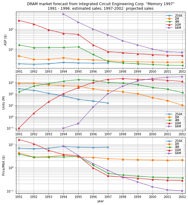
Each generation of DRAM goes through the four classic stages of the product life cycle; here’s what they look like to me on these graphs:
-
Introduction — New and expensive and high-performance. For 16-megabit DRAM this was roughly 1991 - 1995; the price per megabit is higher than the previous generation (4Mb).
-
Growth — Supply becomes more available and the cost has come down enough that it is the most cost-effective on a per-megabit basis. From 1995 to 1997, the 16-megabit DRAM had the lowest cost per megabit.
-
Maturity — Sales peak. The “Memory 1997” projection was for 16-megabit DRAM to dominate sales volumes from 1997-1999, then become overtaken by 64-megabit DRAM but keep selling in fairly high volume.
-
Decline — Sales decline. Why would someone be purchasing a near-obsolete variety of DRAM, when it may be less expensive to buy a better product? Look at the projected prices for 1-megabit and 4-megabit DRAM from 1997 onward: 4-megabit is less expensive! Maybe consumers (like poor old me with my Zeos) need to buy more RAM, but their PC is only compatible with 1-megabit modules. What’s more puzzling, perhaps, is why the DRAM manufacturers keep cranking out their products for 10-15 years after introduction. (Perhaps it’s still profitable and they can keep a small part of their manufacturing line up and running to deliver.)
To put it another way, here’s a then-and-now comparison for DRAMs.
- January 1980: \$65 buys you eight 16-kilobit DRAM chips[67] (Mostek 4116 or equivalent) — that’s 50.8 cents per kilobit, or \$508,000 per gigabit.

- June 2 2022: \$6.62 for DDR4 16 gigabit (2G x 8) 2666 Mbps on the spot market on dramexchange.com,[64] or 41.4 cents per gigabit.

That’s a 1.2 million factor decrease over the past 42 years. If the price of bananas decreased the way DRAM did, you could pay 32 cents for 1.2 million pounds of bananas today. Let me get my shopping cart and try this at the local grocery store....
…nope, didn’t work. I’m trying to imagine a world where the price of DRAM doesn’t decrease relentlessly over time and I just can’t do it.
This is a very rosy picture for consumers of DRAM; all I have to do is wait a year or two and everything gets better and cheaper. But for producers, who have a limited window of opportunity to make a profit from any particular product, it’s a completely different story.
The Remarkably Dramatic Story of DRAM
This seems at first glance like a rather boring industry — yes, there has been some design research involved, but DRAM’s technical challenges are mainly in process engineering: creating a compact bit-storage cell at nanoscale, and repeating it zillions of times reliably and cheaply; as a commodity, customers just want something that works well which they can buy at a reasonable price. But DRAM’s superficial monotony obscures the epic saga of a dynamic business which has had more drama (DRAM-a?), intrigue, and upheaval in the past five decades than European monarchies have experienced in the last five centuries.
Here’s a quick historical summary:
- DRAM with single-transistor MOS cells was invented by Robert Dennard at IBM in 1967. (This is the same Dennard who formulated the rules of Dennard scaling.)
- In 1970, Intel developed the first commercially successful DRAM IC, the 1024-bit Intel 1103 — in case you weren’t aware, Intel was founded as a memory company; microprocessors came later, starting with the 4004 in 1971.
- Throughout the 1970s, US firms had the dominant share of the market. In 1975, Intel led the pack with 46% of the 4Kbit DRAM market, and Texas Instruments, Mostek, and National Semiconductor covering another 42% of it. Japan’s NEC had the largest non-U.S. share of the 4Kbit DRAM market at 4%.[68]
-
Japanese companies gained DRAM market share rapidly in the early 1980s, with support from the Japanese government and electronics companies. These companies learned to achieve higher yields than their U.S. counterparts, and began churning out DRAM chips as if their lives depended on it — which in a way, it did. By February 1982, Japanese DRAM manufacturers had more than 70% of the 64K DRAM market.[69] They kept churning out DRAM, even through a glut and price crash in 1985, which led several U.S. companies to leave the market and pursue manufacturing of EPROM chips instead.[70] 1985 was the straw that broke the camel’s back, and set in motion investigations of dumping,[71] which eventually led to a U.S.-Japan trade agreement on semiconductors.[72] But that didn’t bring back the U.S. DRAM market; in 1987, Japanese firms had seven out of the top ten DRAM producers making up 70% of the market: [68]
Company Market share Toshiba 17.3% NEC 14.1% Mitsubishi 12.0% Texas Instruments 11.0% Hitachi 10.7% Fujitsu 9.2% Samsung 7.1% Oki Electric 4.7% Micron Technology 4.2% Sharp 1.9% -
Korean companies copied Japan’s successes in the 1980s, and gained market share in the 1990s, as Japan witnessed a long recession known as the Lost Decade. Licensing agreements with established semiconductor firms provided Samsung, Hyundai, and Goldstar (later known as LG) with a rapid path to obtain DRAM design and process technology,[73] allowing Samsung to reach the leading position in the DRAM market by 1992, a position which it has maintained most of the time since.[68][74] By the mid 1990’s the three Korean DRAM manufacturers occupied three of the top six market leaders, according to Integrated Circuit Engineering:[66]
Company 1995 share 1996 share Samsung 15.8% 19.1% NEC 11.6% 12.6% Hitachi 10.9% 11.2% Hyundai 8.6% 9.2% Toshiba 9.1% 8.9% LG Semiconductor 7.4% 8.0% TI 7.8% 6.4% Micron 6.1% 6.3% Mitsubishi 5.4% 5.6% Fujitsu 5.1% 5.4% Joonkyu Kang, in a 2010 thesis, includes an estimated ranking of the top twenty DRAM manufacturers for a few different years in the 1990s and 2000s, citing a 2009 UBS publication.[68] Here are the 1995 and 1996 ranks:
Rank 1995 1996 1 Samsung Samsung 2 NEC NEC 3 Hitachi Hitachi 4 Hyundai Hyundai 5 Toshiba LG Semicon 6 TI Toshiba 7 LG Semicon TI 8 Micron Micron 9 Mitsubishi Mitsubishi 10 Fujitsu Fujitsu 11 IBM IBM 12 Infineon Infineon 13 Oki Mosel-Vitelic 14 Motorola Oki 15 Nippon Steel Motorola 16 Matsushita Matsushita 17 Mosel-Vitelic Vanguard 18 SANYO Nippon Steel 19 Sharp SANYO 20 Ramtron Sharp -
From roughly 1998 to 2013, many companies left the DRAM business or were absorbed by other more successful manufacturers. And here’s where things get interesting. I like Lane Mason’s summary of the situation in the May 22, 2009 Denali Memory Report:[75]
The memory marketplace has always invited participation and competition since the earliest beginnings of the semiconductor business in the 1970s. Needless to say, with the memory supplier base becoming more and more concentrated, most of those once-participants no longer make memories today. Caught in the vice of below-cost selling, and an extended period of unprecendented financial losses, we are in the midst of yet another consolidation and elimination phase. Nowhere is this more evident than in the DRAM business. This industry has a ferocious ability to reduce prices and costs (to benefit consumers and expand markets), but it also has Dr. Jekyll’s ability to cause immense financial damage to the greatest of companies, lay waste to reputations, mobilize the resources of huge conglomerates, banks and governments, and surface some of the most confused and spurious arguments for getting into the business, making DRAMs, investing billions of dollars in DRAM fabs and technology, continuing to make DRAMs (and invest in making them) when there is no possibility of ever making a profit, and instead taking suicidal actions to stay in a money-losing business, when those actions only propagate the damage to anyone who remains standing.
…
Although most memory products are highly commoditized, few have caused such financial (and emotional) damage as DRAMs in terms of placing their practitioners in such compromised financial conditions that an exit was a life-and-death choice for the parent or shareholders. Not only is the DRAM business the largest, in terms of revenues, but the large center of the product line…roughly 70-80%…offers almost no room for safe haven, product differentiation, enforced ‘customer (or vendor) loyalty’, or margin protection. Until the advent of NAND Flash, DRAMs were the perpetual leading-edge lithography and technology memory product standard-bearer, pushing the envelope on the litho front ahead of all other products. For a long time, it was said, “You need DRAMs to drive the process technology”, and that was that (at least until Intel said “Logic drives processing”, in the early 1990s.)
Jeho Lee described the DRAM market after 2006 as follows:[76]
Industry fluctuations in the supply of DRAM chips relative to demand have been characterized by what is called “the silicon cycle.” In the period between 2006 and 2008, the DRAM industry experienced an unusually sharp transition from a shortage of DRAM products to an extreme oversupply, culminating with the crash of DRAM prices in 2008. The industry’s overcapacity was preceded by a mad race to expand capacity; this race has been dubbed as the “chicken game” in the media. Even in the time of plunging DRAM prices, players preferred not to reduce their output. The amplified industry cycle accelerated the exit of financially vulnerable firms. I argue that the combination of the amplification of cycle and rising entry barriers fosters the transition of an industry to an oligopoly, in which cyclicality is curbed and the positions of market leaders are solidified.
By the end of 2013, the DRAM market was overwhelmingly dominated by three companies: Samsung, SK Hynix, and Micron Technology.[77] What happened?
One major reason is that the stakes became higher — the cost of state-of-the-art equipment has increased as the technology has improved; new “greenfield” fabs have become much more expensive. DRAM has become quite the high-stakes poker tournament, with increasing costs not only to enter but to remain in the game, and, as the song goes, you’ve got to know when to hold ‘em, know when to fold ‘em, know when to walk away, and know when to run.
But it’s not just a game of poker. There are other nuances of the DRAM market’s upheavals during the past couple of decades.
DRAM in the 1980s
There have been a number of DRAM “crises” over the years, leading companies to exit the business. The DRAM wars of the 1980s, where Japanese manufacturers gained market share, and U.S. manufacturers licked their wounds or walked away, are helpful to provide some context. There were many media articles on the subject; here are some excerpts from three of them. (If you’re interested, read them in their entirety; they provide a good portrait of the issues surrounding the semiconductor industry at the time, many of which are still relevant.)
From the February 28, 1982 edition of the New York Times, a discussion on profitability and the motivation of remaining in the DRAM market:[69]
“I think we’ve already lost out in the 256K,” said W. J. Sanders 3d, chairman and president of Advanced Micro Devices of Sunnyvale, Calif. “The Japanese have won the dynamic RAM market.”
Semiconductor makers are understandably upset, because the dynamic RAM is and will remain the largest selling product in the industry. There are numerous types of semiconductor devices but in computers two main classes are used — memory chips which store data, and logic chips, which manipulate and organize the data and perform calculations.
While logic chips are more specialized, memory chips are churned out like jellybeans. Memory accounted for 27 percent of the 1980 sales of United States semiconductor companies and dynamic RAM’s, which are the main memories used in computers, accounted for 40 percent of all memory revenues.
Last year, the world’s semiconductor industry sold eight million 64K RAM’s, the immediate predecessor of the 256K RAM, and that number is expected to mushroom to more than 700 million by 1985, making the 64K RAM the first product to bring in more than \$1 billion in annual revenues. The 256K RAM, if past precedent is followed, will be an even bigger moneymaker.
But not all American companies are opting out of the race to develop the 256K. Some, such as Motorola and National Semiconductor, are developing the device. The American Telephone and Telegraph Company says it will produce it for its own use starting this fall. There are also many other new products and opportunities in the industry and United States companies still account for two-thirds of the world market. The mere fact that semiconductors are the heart of the exploding computer and telecommunications industries almost assures growth and profits for the companies.
Nevertheless, there is a widespread feeling that the Japanese will dominate the dynamic RAM business in the next two decades. Even if the Japanese do not dominate, analysts say, prices — and the industry’s profits — will come under immense pressure.
“The high profitability of the past is in most cases gone, especially in dynamic RAM’s,” said Daniel L. Kleskin, a semiconductor industry analyst with Dataquest, a market research firm in Cupertino, Calif. “It’s gone forever.”
Pressure is mounting to have Washington do something and the American companies are thinking of teaming up to fight the Japanese. Just recently, top executives of several semiconductor companies and of large computer companies met quietly in Orlando, Fla., at the invitation of the Control Data Corporation, to discuss forming a joint venture for research and development with up to \$100 million in annual funding.
Such dismay is in large part motivated by the stunning victory the Japanese have won in the market for the 64K RAM. American companies knew the Japanese would make a strong play and tried to gear up to meet the challenge. But the Japanese, led by Hitachi, Fujitsu and the Nippon Electric Company, have captured 70 to 80 percent of the market. In the battle, prices have plunged so dramatically that it is thought no company, American, European or Japanese, is making a profit on the 64K RAM.
Some small and medium sized companies, like Mr. Sanders’ \$300 million A.M.D., will have to consider getting out of the market to concentrate on lower volume, more profitable products. Signetics, a company owned by the Dutch electronics company, Philips, pulled out before the 64K RAM appeared.
Because they are produced in enormous volumes, profits from earlier generations of RAM’s have fueled the development of other products and have paved the way technologically to smaller and smaller circuits. Pulling out of RAM’s, therefore, is not an action a company takes lightly.
“If you’re not a factor in memory, you are not a factor in the technology, and if you are not a factor in technology, then it’s only a matter of time before you’re a specialized company,” Mr. Sanders said. Added Andrew Varadi, a vice president of National Semiconductor Corporation, “If you have a large factory and you want to fill it up, you have to participate.”
For that reason, large companies like Motorola, Texas Instruments and National Semiconductor are expected to slug it out for the 64K RAM, the 256K RAM and succeeding generations — such as the 1-million bit RAM — even if they lose money at it.
From the June 16, 1985 edition of the New York Times, similar messages, with a foreshadowing of Korean firms’ entry into the market:[78]
JUST a summer ago, the makers of computer chips rode atop the high-tech world. To supply parts for a seemingly insatiable computer industry, giants like Texas Instruments and Mostek raced to retool their plants for a new generation of memory chips. And three Silicon Valley stalwarts, National Semiconductor, Advanced Micro Devices, and Intel, spent hundreds of millions of dollars adding plant capacity — sure of a quick payback.
This summer, in hindsight, those grand expansion plans look like they were assembled by brash river explorers who discover too late that the noise ahead is Niagara Falls. The industry’s strategy of overcoming Japanese competition with a combination of new technology and greater manufacturing muscle has gone dramatically awry. A huge flow of Japanese-made chips, combined with slow computer sales and wild price cutting from Japan, have plunged American semiconductor makers into their deepest slump ever. More importantly, the downturn has brought permanent damage to one of the few manufacturing industries whose rapid growth had raised hopes of supplanting the declining rust industries.
Even when the slump lets up, experts agree, America will have permanently ceded the biggest single portion of the market to Japan: dynamic RAM’s, the tiny memory chips that store data in electronic equipment of all sorts, from computers to video cassette recorders. Already, several American companies have aborted plans to manufacture the newly-developed 256K RAM’s, which will set the standard for memory chips over the next five years. And only a handful have made prototypes of the next generation of chips — the megabit RAM, four times more powerful. Meantime, half-a-dozen Japanese giants are racing ahead on the megabit RAM.
“The battle in the RAM memory market is over,” John J. Lazlo, Jr., technology analyst at Hambrecht & Quist, said last week. “The Japanese won.”
Boom-and-bust cycles in semiconductors, of course, are hardly new. But for the first time a deep and long depression has been accompanied by remarkable gains in Japanese market share. The big Japanese companies — Toshiba, Matsushita, Hitachi, Mitsubishi and others — are also losing money on chips, of course. But they are more diversified than their American counterparts and they appear willing to absorb the losses, which they are offsetting with Walkmans, televisions, and V.C.R.’s. Their goal is to gain market share and perhaps discourage low-cost Korean producers from entering the memory chip fray.
And from Time Magazine’s issue of October 27, 1986:[79]
The U.S. semiconductor business has seen slowdowns before, but the current struggle has been the worst yet. The problem has its roots partly in the electronics boom of the early 1980s, when sales of products ranging from personal computers to video games created intense demand for chips. Semiconductor makers in Japan and the U.S. vastly increased their capacity, expecting an annual sales growth of 30% to 100%. But when the computer industry’s expansion stagnated two years ago, the resulting glut of chipmakers and chips triggered sharp price cutting. The cost of a 256K dynamic RAM (random access memory) chip, for example, which can store more than 256,000 bits of information, fell from almost \$40 to as little as \$3. Says Andrew Grove, president of Intel: “There are just too damn many of us. It is trench warfare by the commercial armies of two countries.”
By leading the discounting binge, the Japanese have grabbed customers away from U.S. rivals. As recently as 1982, the American share of the global market for integrated circuits, which include the most advanced and widely used types of semiconductors, stood at 49.1%, compared with Japan’s 26.9%. At the end of this year, Japan is expected to have taken the lead with 38% of circuit sales, vs. 35.5% for the U.S., according to In-Stat, an Arizona-based research firm.
Embittered manufacturers in the U.S. contend that Japanese makers have managed this coup by selling semiconductors at a loss, with the aim of pushing their U.S. competitors out of the market. The Japanese chipmakers tend to be diversified electronics giants (the big three: NEC, Hitachi and Toshiba) that can afford to lose money temporarily on semiconductors because they can rely on other revenue to tide them over. In contrast, U.S. chipmakers tend to be specialized, entrepreneurial companies that are more sensitive to profit slumps. An exception is IBM, the world’s largest semiconductor maker, but the computer giant sells none of its chips separately because it uses the entire output in its own products.
The Japanese companies have excelled most of all in the popular dynamic RAM chips, which are used by the dozens in personal computers and by the hundreds in larger models. While this type of integrated circuit was developed in the U.S., Japanese companies have proved adept at efficiently turning them out in mass volumes. Part of the problem is a difference in high-tech corporate culture. Says Richard Skinner, president of Integrated Circuit Engineering, a Scottsdale, Ariz., semiconductor-research firm: “In the U.S., the real glamour jobs are in designing the chips. But in Japan the manufacturing guys are equal.” Indeed, each time U.S. companies have developed a larger-capacity memory chip (first the 1K dynamic RAM, then the 4K, 16K, 64K and now the 256K), Japanese manufacturers have quickly come up with a lower-priced version.
In short:
-
DRAM producers knew that the industry would not sustain a large number of competitors. (There are just too damn many of us.)
-
U.S. DRAM producers framed this competition as a war to be won or lost, and lamented their loss of market share and of profitability. (The battle in the RAM memory market is over. The Japanese won. / The high profitability of the past is in most cases gone, especially in dynamic RAM’s. It’s gone forever. / It is trench warfare by the commercial armies of two countries.)
-
Motivation for semiconductor manufacturers staying in the DRAM market did not just include profitability, but rather technological prowess that could benefit other market segments. (Because they are produced in enormous volumes, profits from earlier generations of RAM’s have fueled the development of other products and have paved the way technologically to smaller and smaller circuits.... If you have a large factory and you want to fill it up, you have to participate.... For that reason, large companies… are expected to slug it out… even if they lose money at it.)
-
1985’s DRAM crisis caught off guard U.S. manufacturers who made big bets that good times would continue, despite business cycles in DRAM being nothing new. (This summer, in hindsight, those grand expansion plans look like they were assembled by brash river explorers who discover too late that the noise ahead is Niagara Falls. The industry’s strategy of overcoming Japanese competition with a combination of new technology and greater manufacturing muscle has gone dramatically awry.)
-
The Japanese DRAM manufacturers were large electronics companies that could sustain losses in their DRAM divisions, but had their own problems to worry about from Korea. (The big Japanese companies — Toshiba, Matsushita, Hitachi, Mitsubishi and others — are also losing money on chips, of course. But they are more diversified than their American counterparts and they appear willing to absorb the losses, which they are offsetting with Walkmans, televisions, and V.C.R.’s. Their goal is to gain market share and perhaps discourage low-cost Korean producers from entering the memory chip fray.)
Japanese DRAM manufacturers continued to lead the market. 1985 was the year of the DRAM glut; 1988 brought on another shortage, even to the point where Motorola just couldn’t help itself and decided to re-enter the DRAM market, and other U.S. manufacturers were thinking about doing so as well, according to an article in the Christian Science Monitor[80]:
For big US chipmakers, not having DRAMs to sell computermakers is “like having a grocery store without a meat counter,” says Juan Benitez, president of Micron Technologies Inc. Micron last week announced a long-term agreement to supply much larger Intel with DRAM chips. Intel, along with a host of other semiconductor-makers, fled the highly volatile DRAM market to invest its energies in more profitable application-specific chips and microprocessors.
The Monitor article went into several reasons why there was interest in re-entering the DRAM market, among them:
- the “home-court advantage” argument:
“It wouldn’t surprise me if US computer manufacturers started favoring US chip suppliers — as long as they get the same quality and the same price as they get from the Japanese,” Mr. de Dios says.
…
Tighter relationships between US chipmakers and US computermakers may insulate DRAM-makers somewhat when the next glut of chips and consequent cutthroat pricing occur.
- the “technology driver” argument:
Because these chips must be manufactured in large volumes at very exacting tolerances, the DRAM is considered a key “technology driver.” Other chips can be technology drivers. But because the DRAM is of a relatively “regular” design, it is a bit easier to pinpoint defects in the manufacturing process.
Fine-tuning a production line to DRAM quality and volume gives a company the superior manufacturing expertise needed to produce lower-volume, more-sophisticated microprocessor chips, and chips for specific applications.
“These processes are very difficult to master,” says Stanley Victor, a spokesman for Texas Instruments. “They require exceptional discipline to manufacture. Making DRAMs drives manufacturing excellence, which, in turn, gives other products a great advantage.”
- the “we take the long view” argument:
Despite the current profitability, chipmakers getting back in the DRAM business have to look to the long run. “You don’t make a decision like that based on market demand at any one time,” says Ken Phillips, a spokesman for Motorola.
Mr. Phillips and others say the money-losing gluts, such as occurred in 1985 and 1986 with the 64K chip, may be less severe in the future. Agreements with the Japanese and closer links between chipmakers and computermakers may act as a buffer, or even defuse future chip gluts. This is because chipmakers are more able, these days, to trust that computermakers’ orders for chips are not inflated.
But wiser observers had warnings about the industry’s cyclical nature.
G. Dan Hutcheson, president of VLSI Research Inc. in San Jose, sees a strong likelihood that past patterns of five-year feast-and-famine cycles will be repeated.
“It’s a textbook case of pure competition,” Mr. Hutcheson says. “It is real easy to overbuild capacity.” This, he says, is due to the long lag time between a corporate decision to build a plant and the 2 years it generally takes to get the plant up to speed. During that time shortages persist, prices are high, and more companies jump on the bandwagon building plants.
“Nevertheless, excess capacity is not right around the corner,” Hutcheson contends. Right now factories are working at 95 percent of capacity and are stretched to their limits. Still, only about 20 efficient plants are needed to supply the world with memory chips, and there are almost that many now. So adding many more plants could lead to a glut in 1 megabit chips, he says.
Shortage, glut, shortage, glut — the wheel turned round and round.... Let’s look at the cycles in a little bit closer detail.
Semiconductor Cycles
Jim Handy listed three causes of semiconductor boom-bust cycles in a 2014 article in Forbes:[81]
-
Capital expenditure fluctuations
-
Process migration issues — consumers want more DRAM in a package, but there are technical hurdles moving to a smaller manufacturing process or a new technology, like the DDR2 → DDR3 transition, that impact available supply. (Another example: the 1988 Monitor article claimed the reason for the DRAM shortage that year was “both US and foreign chipmakers are shifting from 256K (256,000 bits) to 1 megabit (1 million bit) chips and 4 megabit production.”[80])
-
Changes in demand — external economic downturns/upturns, for example; the 2008 financial crisis lowered demand for DRAM.
The last two of these are fairly easy to understand, but the first is subtle, and is the dominant cause of the semiconductor cycle. In particular: (again, from Handy’s 2014 Forbes article)
Capital spending is the big one and accounts for more than half of all cycles, or for more cycles than the other two combined. In a nutshell it’s a predictable sequence: When semiconductor makers are profitable they invest in new manufacturing capacity. This new capacity ramps in about two years to full output, causing an oversupply which unravels pricing. When profits vanish manufacturers shut off capital spending, which later on causes a shortage.
Integrated Circuit Engineering (ICE) Corporation explained the semiconductor cycle similarly:[82]
Swings in production growth rate are closely tied to capacity utilization, ASPs of devices and capital spending (Figure 1-2). For the industry as a whole, when capacity utilization is high, ASPs rise and companies are more profitable, which in turn, encourages capital spending. However, with increased spending, capacity constraints loosen and ASPs tend to drop, decreasing company profitability. The decreased profitability (pre-tax income) then reduces the amount of capital available to invest in future needs.
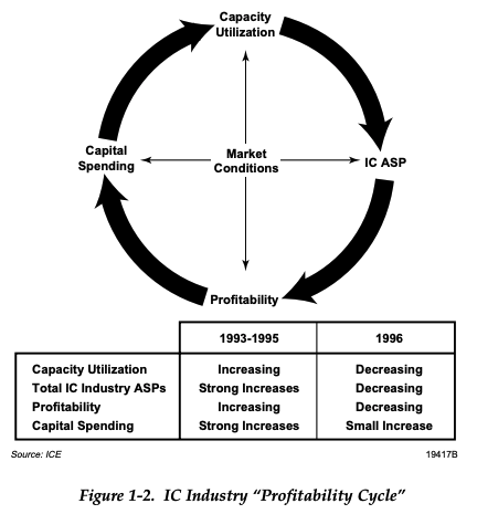
In DRAM, these cycles have taken about four or five years, which you can see in this graph from ICE’s “Memory 1997”:[66]
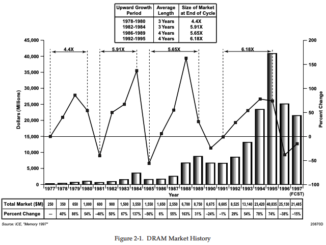
The key issue to understand is that the cycle depends much more on the dynamics of supply, rather than demand. Here’s the number of DRAM units shipped from 1994 - 1996:

There’s a little dip during the first two quarters in 1996, and then recovery in the third quarter, but otherwise, smooth steady growth. If you looked only at the units-shipped graph, it doesn’t seem like there should be much cause for concern.
Meanwhile, during that same time the average sales price dropped to a third of its peak.

Why is the price so volatile?
When semiconductor fabs are so expensive, and rely on economies of scale, there’s not really a middle ground in capital expenditure. Once the trigger is pulled, it takes about two or three years to build — Handy mentioned two years; so did Dan Hutchison of VLSI Research[80]; Paul McLellan mentions examples with TSMC of 22 months and 30 months[83]. So there are these surges in capacity increase, and because fab depreciation is a major chunk of the cost of making chips, the manufacturers will start cranking out as many ICs as they can. Even if the profit is low — or negative! — the choice to churn out new chips is pretty straightforward. The extra cost to run the fab at 90% capacity is only a little bit more than running the fab at, say, 50% capacity. The money has already been spent to build the fab, whether or not they use it.
Let’s say, for argument’s sake — since I don’t have real numbers… I’m looking at ICE’s “Cost Per Wafer”[84] from 1997 for some guidance on relative costs, and making some educated guesses, since fab equipment cost has risen quite a bit — that Mumble Semiconductor has a fab with a full capacity of 200 million DRAM chips during some particular year, with these costs:
- fixed cost of \$700 million in depreciation, for the building and capital equipment
- variable cost of \$1.75 per IC, for labor and materials, as long as they stay between 50% and 90% capacity
And suppose the market for DRAMs this year is not great; Mumble Semiconductor can sell them for an average price of \$6.00.
If it decides to run the fab at 90% capacity (180 million chips), its gross profit will be a paltry \$75 million dollars (6.9% gross margin):
- \$1080 million revenue
- \$700 million fixed cost (\$3.89 per IC)
- \$315 million variable cost
If it decides to run the fab at 50% capacity (100 million chips), its gross profit will be negative, a loss of \$275 million (-45.8% gross margin):
- \$600 million revenue
- \$700 million fixed cost (\$7.00 per IC)
- \$175 million variable cost
So of course the fab decides to run at 90% capacity. Too expensive to idle part of the fab. (Why not run at 100% capacity? I’m just going to handwave a bit for now and say that fabs incur extra costs at high utilization, without really being able to give any explanation. Sorry, that’s just the impression I get.)
Why do the semiconductor companies build more capacity at the top of the cycle?
I’m not really sure, aside from it being an easier expense to bear when profits are rolling in. The contrarian in me says they should be trying to pull the trigger early, so capacity ramps up before the crash — Intel has invested during downturns in 1981[85] and 2008[86] — but I’m guessing that in most cases this is just not possible; by definition, the crash happens when there’s a glut in supply, so as long as the industry undergoes bursts of capacity expansion at the same time, 2-3 years later it will cause a glut and crash when that capacity comes online, gradually becoming more profitable when demand catches up.
Supposedly the semiconductor industry is used to this, and perhaps perpetuates the cycle on purpose, like the Smithore Gambit in M.U.L.E. — even if they don’t resort to price manipulation, they do what they can to take advantage of the swings in price to remain profitable in the long run.
There’s some added complexity here in that the DRAM market is really made up of two pieces:
-
contracts with large computer manufacturers (70-90% of the market[87][88]) — prices are negotiated directly with the DRAM manufacturers, with long-term agreements
-
the spot market — unused chips get sold through brokers on the open market, with supply and demand fluctuating as in M.U.L.E.
The behavior of contract prices and spot prices are slightly different. The spot market is more volatile:[88]
Roughly 70 percent to 80 percent of sales to U.S.-based semiconductor customers are transacted directly with chip manufacturers through long-term contracts. Deals are struck months ahead of delivery. The balance of the chips sold go through distributors to smaller customers and as “spot” sales funneled through an active secondary “gray” market of brokers, distributors, and other arbitrageurs. Spot prices usually rise above contract prices in tight markets, and they fall below contract prices when demand is slack. Thus, to avoid comparing apples with oranges when searching for price differentials, contract prices should be compared with other contract prices, not to spot prices, and vice versa. Dumping complaints have not always drawn these distinctions.
Here are some examples of that volatility. From a 2002 EE Times article:[87]
Alarmist press reports have spread the word for several weeks that DRAM prices are skyrocketing. But take another look.
Virtually all of the price hike data is coming from spot market reports. And indeed DRAM spot prices have been shooting up, according to commodity exchanges.
But OEM contract prices — which comprise 80%-to-90% of all DRAM sales — have remained relatively stable for the last several weeks. Indeed, ICIS-LOR, London-based tracking service, reported that 256-Megabit DRAM prices declined 3.9%-to-4% in Europe and Asia in a 30-day average in June. Sherry Garber, analyst with Semico Research Inc., Phoenix, put the OEM price drop of 256-Mbit in June at an even steeper 17%. Just this week, however, reports from Korea indicated a small uptick in DDR contract prices.
And a 1988 Computerworld article:[89]
According to some reports, 256K-bit DRAM chip contract prices have dropped from 20% to 40% in the last two months, with 1M-bit contract prices falling nearly 20%. Chip prices have begun to decline as more manufacturers bring 1M-bit manufacturing capacities on-line, easing the need for the older-generation 256K-bit chips.
“In general, there has been a certain easing on the availability,” said Albert Wong, cofounder and executive vice-president of advanced technology at AST Research, Inc. in Irvine, Calif. AST was forced to pay spot prices — noncontract prices that do not give the buyer the benefit of long-term contract pricing — on several occasions this year to make ends meet, Wong said.
In addition to serving customers who are willing to live with that volatility, the spot market has other institutional advantages:[90]
In the semiconductor industry, for example, e-marketplaces like Converge support an active spot market for dynamic random-access computer memory devices (called DRAMs). Major buyers and suppliers conduct the majority of their transactions through negotiated contracts, using spot markets primarily to buffer supply and demand shocks. In addition, spot markets enable contract prices to adjust more rapidly to shifts in supply and demand because they serve as a benchmark during contract negotiations. They also improve resource allocation by serving as an important input for suppliers evaluating potential investments in new production capacity.
Beyond that, I don’t really know how to characterize the spot market, which is really just applicable to memory like DRAM and Flash, because of their near-commodity status, and not something that occurs with most other semiconductor products. Somehow, in my head, I picture a small, nondescript office building in Jersey City, where some guys named Ernie and Izzie left Crazy Eddie’s in the mid-1980s, before it went bankrupt, and started a gray market for DRAM, trading orders while eating lots of pastrami sandwiches… and perhaps it became computerized at some point. But I suspect that mental image is incorrect. (Jim Handy answered a question of mine on this topic, and tells me he had known a few individuals in the spot market, making phone calls on their own, to prospective buyers and sellers on their contact list.)
Because of the continuing decrease in DRAM prices over time — Moore’s Law — there is a high incentive for anyone holding DRAM inventory to find a buyer sooner rather than later. I’m not going to want to hold onto a product that loses 20-30% of its value each year, even if you average out all the swings due to volatility.
So, in summary, these kinds of issues — the high capital expenditures, the commodity status and the spot market, the decrease in value over time — along with the large number of producers, seem to lead to a couple of behaviors that affect price, as best as I can tell:
-
DRAM manufacturers choose, in effect, the quantity of product they produce, two to four years in advance, when they make decisions on capital expenditures. After they build a new fab or update the production line, they don’t have much choice but to churn out most of what their plants can supply, regardless of the price. (This price-independent nature of quantity is called an inelastic supply in economic-speak.)
-
If there are a large number of producers in the market, each with a small share, the manufacturers have almost no control over price. Remember the trading line in M.U.L.E.: if a DRAM manufacturer raises their price significantly, it means they will lose market share, because their customers will move to someone else in the market willing to sell for less, or to the spot market.
-
The high cost and long delay of capital expenditures means that even the control over quantity produced is very coarse, and a risky prediction.
-
The cyclical nature of the business means that prices will zoom downwards after a bunch of capacity spending, ruin profits for a couple of years, and then, if these manufacturers are lucky, the ones with the highest profitability margin and high market share will recoup their investments and be ready to gamble on another round.
Does anyone still want to play?

Indianapolis Times, October 5, 1928
Dance Marathon, with Bears
The last two major DRAM crises led to the exit of all of the major DRAM manufacturers outside the Samsung/SK Hynix/Micron triumvirate. One was during the dot-com bubble in 1997-1999. The second seems more interesting to me: the 2006-2009 DRAM crisis began with a very profitable year of 2006 across the industry, with a surge in demand for PCs and a shortage of DRAM chips.[76] Why would that be a bad thing for DRAM manufacturers? It sounds much like the chip shortage of today; when demand is high and we can’t get enough supply, the price goes up, manufacturers take profits and enjoy them while they can. Aside from benefiting shareholders, when chipmakers are flush with cash, that’s the time to invest in new capital expenditures, because the good times will inevitably come to an end. In 2006, the end was hastened by an overestimation of DRAM demand caused by the release of Microsoft Windows Vista.[91] (OS upgrade? Haha, you’ll need more RAM!)
The stage was set, and like the dance marathons of the 1920s and 1930s, some of these players had to drop out, one by one.
Semiconductor capital expenditures have a couple of positive impacts:
- Increase in supply.
- Decrease in cost per transistor.
- Technological advantage.
The DRAM companies knew all of this, and were forced to spend money, whether they wanted to or not. Jeho Lee describes it this way:[76]
Since industry participants have largely competed based on price, they have been willing to move quickly to whatever state-of-the-art, process technology (often possible with the latest manufacturing tools) that minimized the cost per bit, or the per-unit cost of computing power. As a consequence, DRAM manufacturers have continuously pushed the frontiers of technological possibility, and the DRAM business has long been viewed as a technology driver.
What would happen if a DRAM manufacturer chooses not to follow this cost reduction game? Once the industry starts the mass production of the new generation chips, their price tends to drop dramatically within a few years. For example, the price of a 4-megabit DRAM chip was around \$40 when industry leaders first began producing chips in large volumes. Within four years, however, the price dropped to about \$2. Unless DRAM manufacturers matched such dramatic cost reduction at a later stage of the industry cycle, they were unable to survive (West 1996; Shin and Chang 2008). Even industry leaders were not exceptions to this ruthless selection process. For example, Intel exited the industry when it could not narrow the cost gap with Japanese DRAM manufacturers in the 1980s. In the 1990s, the Japanese leaders followed in the footsteps of Intel, as Samsung overtook the industry leadership, aggressively driving down the cost per bit.
DRAM manufacturers should have learned that the name of the game in order to survive in the industry is to drive down the cost per bit faster than the competition. Cost reduction can be achieved by increasing capacity to realize economies of scale or by reducing the cost per bit with the latest process technology. As a consequence, the pressure to survive appears to have led DRAM manufacturers to develop an obsession with economies of scale and process innovation, which, in turn, resulted in a massive buildup of products leading to overcapacity and aggressive migration to new process technologies in the face of mounting losses.[76]
Supply increases. Costs decrease. A 1976 article in Business Week — back then, the dominant DRAM size was 4 kilobit — described the situation more bluntly:[92]
“The frightening thing in this business is that if you’re not first—or a fast second or third—you’re in trouble,” says Robert R. Heikes, No. 2 man at Motorola Semiconductor. And Bernard V. Vonderschmitt, head of RCA Corp’s Solid State Div., adds, “If you come in a year late, you’d better have a much improved version or a new process that permits you to make the product more cheaply.”
By being first on the market, a semiconductor manufacturer can build up production rates faster and advance down the “learning curve”—the industry principle that says that as production doubles, experience and higher yields of good parts will drop manufacturing costs by 27%. Thus, the first company to deliver a new product in high volume can drop its price fastest and retain the largest market share.
The companies who do better at reducing costs gain market share and can be more profitable than the ones who don’t. And “more profitable” in a DRAM capacity expansion arms race really means “less unprofitable”. When the supply increases, the price of DRAM drops, and boy did the bottom drop out of the DRAM market in 2007.
Kang’s 2010 thesis[68] includes the following graph of profitability during this crisis:

Survival was not only a matter of financial strength, but endurance.
Basically it’s like that joke where one guy asks another why he starts putting his running shoes when they come across a bear that they both know they can’t outrun; the one with the running shoes says “I don’t have to outrun the bear, I just have to outrun you.”
The bear here is the threat of insolvency, and the insidious part of the DRAM market, especially during 2006-2007, is that DRAM manufacturers had a Kobayashi-Maru-style choice:
- Invest boldly in capital expenditures, where no one has gone before, in an attempt to become more profitable than the other firms in the future (“I don’t have to outrun the bear…”)
- Invest only cautiously in capital expenditures, to conserve capital and attempt to ride out the inevitable crisis. But the 512 megabit DRAM chips of 2006 would be obsolete in a few years, and future profits would be doomed. The bear’s pace is set by the leading-edge manufacturers, who are willing to endure this roller coaster ride of profitability.
A 1993 article, “The Risk of Not Investing in a Recession” delves into this dilemma:[93]
Two very different ways of thinking about investment and risk are headed for a showdown. One emphasizes the financial risk of investing; the other concerns the competitive risk of not investing. In normal times, the bearishness of the former tends to (or is supposed to) complement the bullishness of the latter. But the balance between the two seems to break down at business cycle extremes. Specifically, at the bottom of the business cycle, companies seem to overemphasize the financial risk of investing at the expense of the competitive risk of not investing.
The article cites DRAMs in the mid-1970s recession:
When the downturn hit, U.S. competitors mostly deferred their investment in capacity to produce 16K chips, but their Japanese rivals didn’t. When the upturn came, IBM and other U.S. customers, unable to source 16K DRAMs from domestic suppliers, began to turn to Japanese suppliers for the first time. This shifted the balance of trade in semiconductors to favor the Japanese, who, by 1979, had captured 43 percent of the U.S. market for 16K DRAMs. They have never looked back, with the result that there is virtually no U.S. merchant supply of DRAMs today. Failure to invest in time proved fatal in this segment for three related reasons: its very fast growth, the opportunities that it afforded for rapid yet relatively cumulative technological progress, and customers’ willingness to switch vendors if that was necessary to secure improved (next generation) chips. Note, by the way, that the critical failure occurred after the economy had bottomed out, that is, during a general recovery.
Lee’s article points out some other key reasons why the 2006-2009 crisis led to overcapacity and a winnowing out of less-profitable DRAM manufacturers:
-
The switch from 200mm wafers to 300mm wafers — a step function in productivity was about to occur. Some steps in the IC fab process occur one wafer at a time, and by jumping from 200mm to 300mm wafers, the throughput of those steps more than doubled. Same number of wafers per hour, but now there are around 2.25× the number of die on each wafer. (Upgrade, upgrade, upgrade!) Those manufacturers which invested in 300mm wafer equipment would get a large boost in profit margin in the long term, as long as they were able to afford a large investment in capital equipment.
-
The 2008 financial crisis — Pretend you’re a DRAM manufacturer. In 2006 the bank lends you a bunch of money so you can execute your capital expenditure strategy. Now it’s 2008 and not only is there a glut of DRAM from 2007, but now the subprime mortgage crisis is ruining world economies and consumer demand drops further… oh, and by the way, the bank just called and wants its money back; it has bigger problems to deal with. That loan makes you look like Mr. Foolish right about now.
Or, perhaps you were running a fiscally prudent operation, and had no long-term debt in 2006 or early 2007. But here it is 2008, and your operating margin has been negative for a few quarters, and you’re a sinking ship trying to stay afloat, so you manage to secure a loan to keep the lights on, hoping to ride out the storm. Are you Mr. Foolish?
I would like to add one more:
-
DRAM and other memory processes are highly specialized. The name of the game is about reducing cost and maintaining profitability. This has driven memory manufacturers to use different mixes of tools and different process geometries than other leading-edge semiconductor manufacturers (CPUs, high-end ASICs, etc.) — news articles and financial releases of DRAM companies have talked about various weird technology nodes like 80nm and 78nm and 73nm, whereas the more common industry nodes are in roughly square-root-of-two steps (180nm, 130nm, 90nm, 65nm, 45nm, for example). This means memory manufacturers are much less able to rely on foundries than other parts of the semiconductor market, and are on their own, as an integrated device manufacture (IDM), for capital equipment investments. (Most of the characteristics of the DRAM market also apply to other memory markets, like NAND Flash, which is ubiquitous in USB flash drives and SD cards.) A recent summary of the semiconductor industry put this as follows:[94]
DRAM technology nodes (the production line in a fab) have very short lifetimes, and profitability requires maintaining pace with the technology leader Samsung. Therefore, all DRAM vendors operate as IDMs.
Okay, enough of the abstract discussion. I’d like to take a different perspective.
I showed this graph of profitability ratios in a recent article:

Micron Technology (MU) doesn’t look like it’s doing very well in this period, with the worst gross margins of this group of twelve, and poor operating margins. But Micron is the only memory manufacturer in the group, and in retrospect, it doesn’t seem fair to show this graph without some context. (Another disclaimer: this article is not intended as financial advice.)
So we’ll look at the change in the DRAM market over time a different way, with some focus on the fab that Micron Technology started constructing in Lehi, Utah in July 1995. The Lehi fab has a somewhat colorful history. It reminds me of Charlie Brown trying yet again to kick the football before Lucy pulls it away from him, or perhaps of Scarlett O’Hara’s moment of determination in Gone With the Wind: “As God is my witness, as God is my witness, the Yankees aren’t going to lick me. I’m going to live through this, and when it’s over, I’m never going to be hungry again.”
Ahem.
At any rate, as you read this section, think about some of the financial decisions that have been made involving semiconductor fabs, and where they fall in the Mr. Spendwell / Mr. Frugal / Mr. Foolish classification. Also, we’re going to keep track of how many players are left in the game from the top eighteen DRAM manufacturers in 1996. (I would have tracked the top twenty, but the bottom two, Sharp and Sanyo, seem to have quietly disappeared from the DRAM business with no indication they ever left.)
Oh, and it’s time for some music; here’s some Genesis from 1983:
Here we go:
-
October 18, 1994 (Lewiston Tribune, Oct 19 1994) — Micron Technology announces it will build a \$1.3 billion manufacturing plant, comprising roughly \$491 million for land acquisition, site preparation and construction, and \$820 million for equipment, at a site to be determined. (In an odd coincidence for this article, Micron announced the same day that it was acquiring Zeos.)
-
March 13, 1995 (Deseret News, Mar 13 1995) — Micron selects Lehi, Utah.
The Micron plant will consist of four separate buildings, each about 250,000 square feet and costing about \$125 million. Total construction costs will be about \$490 million, and Micron will spend another \$800 million equipping the buildings.
-
July 1, 1995 (Deseret News, Jul 1 1995 — Micron breaks ground on its new plant in Lehi.
The Boise-based company has apparently chosen a good moment in the volatile semiconductor age to double its production capacity. Micron reported record third-quarter earnings in June that more than doubled totals for the same period last year as demand for its primary computer chip remained strong and production skyrocketed. The memory chip market is expected to triple to \$90 billion annually in four years. Semiconductor fabrication plants are nearly maxing out, running at 94 percent capacity worldwide.
-
August - October 1995 (Deseret News, Feb 27 1996) — Cost of Lehi plant increases to \$1.7 billion and then \$2.5 billion
-
First quarter 1996 — the price of DRAM starts dropping precipitously as new industry capacity comes online. Remember this graph I showed from ICE’s “Memory 1997”?[66]
DRAM manufacturers must look back fondly upon 1994 and 1995 when everything was up, up, up! There was no end in sight to the outstanding growth—until 1Q96. As noted in the chart, average selling prices fell steeply and fell quickly.
Dataquest had this to say about DRAM in March 1996:[95]
Dataquest forecasts continued DRAM price declines throughout 1996 as a direct result of the large amount of DRAM fab capacity that continues to come to market (especially for the 16Mb density). Our forecast shows that contract pricing for DRAM dropped an average of 30 percent from the fourth quarter of 1995 to the first quarter of 1996.
-
February 26, 1996 (Deseret News, Feb 27 1996) — Micron announces it will “delay completion of its new \$2.5 billion Lehi memory chip manufacturing plant until the market improves. Work on the plant’s shell will end in six to eight weeks. Micron already has spent \$400 million on the plant and will pour another \$100 million to \$200 million into the facility before work wraps up. As many as 40 employees Micron has already hired for the Lehi plant will be offered positions in Boise, company officials said.”
-
June 5, 1997 (Deseret News, Jun 5 1997)
Micron announced Wednesday it will employ 200 to 300 people at the Lehi plant next summer to test memory chips made at its Boise facility. Jobs to be filled include test production operators, technicians and engineers.Micron spokeswoman Julie Nash said the test facility is one of three operations originally planned for the \$2.5 billion structure. “We will not put the rest of the facility under a more aggressive schedule until we see more sustained strength in the market,” she said.
Just as I thought it was goin’ alright
I found out I’m wrong, when I thought I was right
-
July 1, 1997 — Motorola announces it will exit the DRAM business. An article by CNET states that Motorola was “making good on its promise to abandon underperforming efforts.”
“Motorola was making DRAMs to round out their product portfolio. They had no proprietary technology and little investment,” said Jim Handy, an analyst with Dataquest. “They don’t need DRAM to succeed.”
The transition will not take place overnight. Motorola’s DRAM production comes out of two joint ventures with, respectively, Toshiba and Siemens. Motorola will phase out their own DRAM production at the plant co-owned with Toshiba in Sendai, Japan, by the end of the year and convert the resulting plant capacity to make logic products next year. Toshiba will continue to make DRAM chips at the plant.
By contrast, the Motorola-Siemens joint venture based in the White Oak Semiconductor facility in Richmond, Virginia, will actually only start to make DRAMs by mid-1998, said Ken Phillips, a spokesperson for Motorola. The plant is under construction, he said, and will manufacture DRAM chips to ramp up production. DRAM production will continue until early 2000, when manufacturing of fast memory chips will take over.
-
March 3, 1998 (EE Times, Mar 4 1998) — TI and Acer end their joint DRAM venture; Acer purchases full ownership, renames it Acer Semiconductor Manufacturing Inc. (ASMI), and shifts to a combined foundry-DRAM model. TSMC will eventually buy part of ASMI and then all of it by the end of 1999, presumably completing a shift from DRAM to foundry.
-
June 18, 1998 (EDN, Jun 19 1998) — Micron and Texas Instruments announce an agreement for Micron to acquire the remainder of TI’s memory business, including fabs, in exchange for around \$640 million of Micron stock and the assumption of \$190 million of TI’s debt.
-
September 1998 (Seattle Times, Sep 9 1998) — Matsushita (known outside Japan through its Panasonic brand) announces it will end its U.S. operations, consisting of a DRAM plant in Puyallup, Washington.
-
September 1998 (EE Times, Sep 24 1998) — Hyundai Electronics and LG Semicon (#4 and #5 in the 1996 list) agree to merge, but disagree about who gets control over the combined operation. Four months later, in January 1999, the two companies finally reach an agreement that Hyundai Electronics will retain control. (South Korea has chaebols, which are basically corporate industrial conglomerate fiefdoms. Imagine if Coca-Cola and Dell Computer and Walgreens and John Deere and Dow Chemical were all part of one big company, run as a family business, and there were a few dozen of these sorts of groups, and that nobody outside the country really understood why things work this way. At least that’s my impression of it.) Hyundai Electronics will change its name to Hynix Semiconductors in 2001 and SK Hynix in 2012.
-
September 30, 1998 (EDN, Sep 30 1998) — Oki Electric ends plans to produce 256-megabit DRAM; Oki’s president expects the company to phase out DRAMs sometime in 2000. (I can’t find a definite announcement of a DRAM exit, though; as of October 2001 Oki was still producing DRAMs but at that point let’s just call it a dead business walking.)
-
September 30, 1998 (EE Times, Sep 30 1998) — A majority share of Nippon Steel Semiconductor is acquired by United Microelectronics, which will shift manufacturing from DRAM to foundry operations.
-
October 1, 1998 (EDN, Oct 1 1998) — Micron completes acquisition of TI’s memory business, under a somewhat different deal tha originally announced:
TI has received approximately 28.9 million shares of Micron stock valued at \$881 million, \$740 million in notes convertible to an additional 12 million shares of Micron stock, and a \$210 million subordinated note. The market value of the convertible and subordinate notes is approximately \$836 million. In addition, Micron received \$550 million in proceeds from financing providing by TI to facilitate the deployment of Micron’s technology throughout the acquired business, and Micron received a 10-year royalty-free cross license agreement.
-
January 11, 1999 (EE Times, Jan 11 1999) and (Electronics Weekly, Jan 20 1999) — Fujitsu announces it has no plans to leave the DRAM market, denying a report from Japan’s Nikkei Keizai Shimbun newspaper.
-
March 14, 1999 (Deseret News, Mar 14 1999) — Lehi plant still not open, four years after the original site selection.
Some 2.3 million square feet of buildings sit largely empty, save pallet upon pallet of floor tiles, lights and other interior fixtures waiting for installation someday.
About 175 people work at the plant in various capacities from maintenance to information systems to engineering. None are doing what the massive plant was built for, making computer memory chips found in nearly every electronic device imaginable.
The facility isn’t equipped to manufacture anything. The company scrapped plans last year to bring in equipment and hire 400 workers to test chips that were made in Boise.
Micron remains mired in the longest and worst market slump the semiconductor industry has seen. Like Geneva Steel a few miles south on I-15 in Utah County, the company has suffered from a flood of low-priced foreign imports. Computer memory chip prices have fallen 97 percent the past four years. The \$3.75 Micron used to take in for each megabit of memory it created nose-dived to 16 cents per megabit.
…
Micron doesn’t intend to pack more than a billion dollars worth of manufacturing equipment into the Lehi facility without a steady upturn in the roller-coaster market. “Until we see that, we’re going to keep the dollars pretty close to the vest,” Bedard said.
Nevertheless, Micron bought Texas Instruments’ memory operations last September and interest in production facilities in Japan, Italy and Singapore. Those acquisitions give rise to the question, why not expand in Lehi instead?
The answer is simple, Fuhs said. Micron isn’t going to invest in a new project until the ones it has are at full capacity. “They get more bang for the buck in those operating concerns,” he said.
-
April 1999 (Electronics Weekly, Apr 7 1999) — Matsushita will leave the DRAM business for PCs, continuing only to make some DRAM for its own consumer electronics division.
-
July 1999 (EE Times, Jul 8 1999) — IBM announces it will sell its stake in Dominion Semiconductor, a joint DRAM venture with Toshiba, effectively getting out of the commodity DRAM business.
-
November 29, 1999 (EDN, Nov 29 1999) — NEC and Hitachi (#2 and #3 in the 1996 list) announce they will merge their DRAM operations as a joint venture; in 2000 they pick the name Elpida.
-
December 1999 (EDN, Dec 13 1999) — Fujitsu announces it will phase out commodity DRAM production; its facility in Gresham, Oregon will shift “to flash and logic production next year.”
Are you keeping track? We’re down to 9 out of the original 18, with these departures and mergers:
- Motorola
- TI
- LG + Hyundai → Hynix
- Oki
- Nippon Steel Semiconductor*
- Matsushita
- IBM
- NEC + Hitachi → Elpida
- Fujitsu
*wait, Nippon Steel?! Conglomerates sometimes include some bizarre attempts at “diversity” or “synergy”. International Rectifier got into the antibiotics manufacturing business in the early 1960s, but exited in the mid-1980s after a lawsuit. Long Island Iced Tea Corp decided to get into the blockchain business in 2017; this strategy did not appear to end well.

Indianapolis Times, October 9, 1928
-
November, 2000 (Lewiston Tribune, Nov 19 2000)
Micron plans to begin a prototype chip plant on 12-inch wafers. “During a Webcast discussion with Wall Street analysts, Micron Chairman Steve Appleton said the company intends to set the Lehi plant up to begin manufacturing Dynamic Random Access Memory chips on 12-inch wafers, rather than the eight-inch wafers the company now produces, according to Bloomberg News Service. The plant should be in production by the end of next year.
-
February, 2001 (EDN, Feb 23 2001) — Nope, more delays.
Micron Technology Inc. last week halted plans to equip a 300-mm-wafer pilot line at its Lehi, Utah, fab, which was to have begun this quarter, and will “wait on market conditions” before deciding when to go ahead, a spokeswoman said.
The company attributed the decision to a slowdown in the chip market, which caused it to delay equipping a pilot line at the first of several fab shells at the Utah complex. When the memory market improves, “it would then be prudent to start installing production systems for a 300-mm pilot line,” the spokeswoman said. Micron had told investment analysts earlier this month that it was starting to equip at least two 300-mm pilot lines. That work has been largely put on hold, although the company will complete some early work to prepare the lines, the spokeswoman said.
Micron, Boise, Idaho, completed the Lehi fab shells years ago, but they were mothballed about five years ago during a downturn in the DRAM market. The spokeswoman said since the shells already exist, once Micron starts installing production gear, the fabs can be brought into production relatively quickly.
I could leave but I won’t go
But it’d be easier I know
I can’t feel a thing from my head down to my toes
-
November 29, 2001 (EDN, Nov 29 2001) — Fujitsu announces it will close its Gresham, Oregon facility.
Established in October 1988, the Gresham plant was Fujitsu’s first overseas wafer fabrication facility and has served as one of its key production bases for memory products. In April 2000, based on Fujitsu’s strategic withdrawal from commodity DRAM production and robust demand for flash memory devices, the Gresham plant began converting all production lines to flash memory. However, due to the precipitous and prolonged downturn of the flash memory market since the beginning of this year, the plant has been operating at levels well below capacity, the company said.
-
December 2001 (EE Times, Dec 18 2001) — Opportunity knocks for Micron, when Toshiba announces it’s exiting the DRAM business, and what do you know, there’s a fab in Virginia up for grabs:
Micron Technology is believed to be offering between \$250 million and \$400 million in stock to acquire Toshiba Corp.’s Dominion Semiconductor fab in Manassas, Va., according to reliable sources close to the negotiations.
The final financial amount and full details of the deal are yet to be worked out, since the two chip makers Tuesday only signed a memorandum of understanding. However, one informant said Micron is expecting to acquire the leading edge 0.17-micron processing fab for a quarter of the \$1 billion to \$1.2 billion cost of building a similar new fab from scratch.
-
January 2002 (CNET, Jan 2 2002) — Matsushita announces it will stop producing DRAM altogether. (It had exited PC DRAM in 1999.)
-
July 2002 (EDN, Jul 9 2002) — Manufacturing lines for 300mm wafer DRAM are under construction at the former Toshiba/Dominion Semiconductor fab in Manassas.
-
October 2002 (EE Times, Oct 3 2002) — Mitsubishi’s DRAM business will be acquired by Elpida.
This leaves seven out of 18 from the 1996 DRAM list, with Elpida the only remaining Japan-based DRAM manufacturer.
-
December 2002 (New York Times, Dec 11, 2002) — Infineon announces it will get out of its stake in ProMOS Technologies, a joint DRAM venture with Mosel Vitelic, alleging a breach of contract. (EDN states it more bluntly: “ProMOS Technologies is a joint venture between Mosel and Infineon, but its parents appear about to undergo a messy divorce.”)
-
March 2003 (Deseret News, Mar 6 2003) — Lehi: Still nope.
“Our business is cyclical in nature and will continue to be,” said Kipp Bedard, a Micron spokesman. “With that in mind, Lehi continues to be on our road map for future expansion.” Bedard said the computer industry was surprised and dismayed when sales took a dive and orders for computer memory wafers slowed shortly after Micron started work on its proposed \$1.3 billion building on a Utah County hillside.
Instead of employing between 3,000 and 4,000 workers, Micron has consistently run the Lehi testing plant with only a few hundred. Instead of holding a splashy dedication ceremony a year after breaking ground, the company has quietly inched along constructing the 900,000-square-foot set of buildings without fanfare.
Truth is I love you more than I wanted to
There’s no point in tryin’ to pretend
There’s been no one who makes me feel like you do
Say we’ll be together ‘til the end
-
December 2003 (Wall Street Journal, Dec 1 2003) — Vanguard International Semiconductor’s chairman Paul Chien announces the company will leave the DRAM business by mid-2004, to focus on its foundry business.
Mr. Chien said Vanguard’s decision had a lot to do with a gross profit margin in the foundry business that is “currently close to 29%.” In DRAM, “there really is no gross margin — it is barely breaking even,” he said.
-
December 2003 (Taipei Times, Jan 6 2004 — Mosel Vitelic sells its DRAM business to ProMOS Technologies. This isn’t covered well in the media; Kyung Ho Lee’s 2013 thesis[96] cites a June 2012 Gartner report that mentions Mosel Vitelic’s DRAM exit was in 2004, and there are articles citing both 2004 and 2006 as Mosel Vitelic’s departure from DRAM. In August 2011, ProMOS itself announced it would be exiting the DRAM business, also a sparsely covered story. If a DRAM manufacturer exits the business and no one is there to hear it, does it still make a sound?
-
May 2004 (Deseret News, May 12 2004) — Better economic times in the DRAM industry:
Lockhart said the Lehi facility remains focused on testing product that has been fabricated, probed and assembled in other Micron plants.
The job force currently stands between 500 and 600 workers, he said. They have been hired to do technical work at a better-than-average entry-level wage.
“Our Lehi facility is still on the road map and was built with 300 mm wafer technology in mind,” Parker said. “Job growth and utilizing more of the building’s capacity are dependent upon market conditions, which we evaluate on a regular basis.”
Only about 30 percent of the 2.3 million-square-foot Micron building is in use. The world’s second largest maker of computer memory chips is upbeat as memory chip prices have firmed, according to a Reuters news service report out of Singapore.
By November 2004, with the loss of Mosel Vitelic and Vanguard, we’re down to 5 out of 18 from the 1996 DRAM list, leaving these contenders with a combined 82.5% market share, according to iSuppli:
- Samsung (29.8%)
- Micron (15.9%)
- Hynix (15.5%)
- Infineon (14.3%)
- Elpida (7.0%)
Hang on tight....

Indianapolis Times, October 25, 1928
-
November 2005 (Deseret News, Nov 22 2005) — Micron and Intel announce a joint venture, IM Flash, to make NAND flash memory, with Lehi eyed for possible production:
Micron has invested about \$1 billion so far in the Lehi plant, which originally was designed for manufacturing but now has 500 workers involved in chip testing.
“If all goes well… our test employees will transition to manufacturing NAND flash… We would see a transition over time, and that would mean in 2007 we’ll see some additional investment in the facility from a construction perspective — again, if everything goes the way we’re envisioning,” said Trudy Sullivan, a Micron spokeswoman.
-
January 2006 — the New York Times (Jan 21 2006) reports that Infineon will spin off its memory chip business some time in the near future, quoting its chief executive, Wolfgang Ziebart, in a question-and-answer format:
Q. And the latest step is now to shed that commodity memory business. Why didn’t you do it a year ago when DRAM was in the profitable part of its business cycle?
A. You could do it when pricing is more favorable, which it was when I came, but the shape the company is in is at least as crucial as the market itself. The DRAM cycle itself is stronger than the differences between the players. Even the best player might be in losses in the downturn and even the worst might be in profits in the upturn. What’s important is to perform better than the competition over a full cycle. One year ago, relative to our competition, the company was in much worse shape. We were lagging behind in the technology at the time. The best in technology is Samsung. We were six months behind. We’ve reduced that to three months. We’re confident we’ll be able to close that gap as we move to chips with smaller circuitry.
-
March 2006 (Deseret News, Mar 18 2006) — Lehi is a go: IM Flash announces it’s putting its headquarters in Lehi!
IM Flash Technologies LLC on Friday said it will hire 1,850 people in Utah over the next two years and put its corporate headquarters at the former Micron Technology Inc. facility here.
David Simmons, chairman of the Governor’s Office of Economic Development Board, said the IM Flash investment in Lehi — \$3 billion to \$5 billion — represents the largest single business investment ever in the state.
-
March 31 2006 — Infineon puts out a press release announcing its memory spin-off of Qimonda, will take place in May:
Infineon Technologies AG (FSE/NYSE: IFX) announced today another milestone in its strategic realignment. The carve-out of its memory products business group into a new company will be effective on May 1st, 2006, two months ahead of schedule. On that date, the new company named Qimonda will start its operations. Qimonda, headquartered in Munich, will have the legal form of a German Aktiengesellschaft (AG). The new company will initially remain a wholly owned subsidiary of Infineon. It is the clear intention of Infineon to launch an Initial Public Offering (IPO) of Qimonda as the preferred next step. The separation on organizational and technical levels has made quick progress, enabling Infineon to carve out Qimonda earlier than it had originally planned.
-
August 8 2006 (EDN, Aug 9 2006) — Qimonda’s IPO raises less than expected.
At a press conference in New York City Wednesday morning Qimonda and Infineon officials conceded the market environment has been difficult, with almost half of the planned IPOs since July 1 withdrawn from the marketplace. But they insisted there were no plans to shelve the IPO.
-
February 2007 (Deseret News, Feb 18 2007) — The Lehi facility is described as “a bustling hive of engineers, production employees, contractors and others working on a scale unprecedented in the state’s history.”
That activity is in stark contrast to what for years served as a massive monument to the foibles of the marketplace. Started in the late 1990s for Micron Technology to produce computer chips, the seven-building Lehi complex saw construction halted when the chip market sank. Dreams of the \$1.3 billion plant employing about 3,500 people — which Micron said in 1995 it someday would — instead morphed into 2.3 million square feet of dormancy. Micron was able to move some chip-testing operations there, but, at tops, it had only 500 workers — nothing to sneeze at, but far short of those initial projections.
…
Construction is expected to continue for about another year. About 60 sophisticated tools are being added each month, each costing between \$1 million and \$28 million and about \$300,000 just to install.
The tools and employees are busy producing 12-inch wafers, each containing about 300 fingernail-size die (lay people would call them “chips”) of NAND flash memory that will be used in consumer electronics, removable storage and handheld communication devices such as mobile handsets, digital audio players, digital cameras and GPS navigation devices. Around-the-clock shifts will eventually churn out up to 2,000 wafers per day. The company expects to have a ceremony this week to mark the first wafer out of the plant. All products will go to Micron and Intel to market, although Apple worked out a deal to get \$500 million of inventory.
Lehi is one of only two plants in the country, the other being in Virginia, producing NAND flash.
“This plant is being developed to compete on a global scale with Samsung and Toshiba, as well as other competitors,” [IM Flash spokeswoman Laurie Bott] said. “And NAND flash is going to affect anyone who has an iPod, a security system, digital camera, video camera or car computer because of no moving parts, portable power and memory.”
But processing NAND flash is no simple task. Each wafer goes through 400 to 500 processing steps, sometimes going through one of the high-tech tools up to 100 times. The steps can take as little as 10 minutes or up to six hours.
-
February 2007 — An article in the Feb 26 2007 edition of EDN describes a “perfect storm” as all three of Micron’s business segments are in a downturn. This article points out a capacity-planning dilemma:
Currently, Micron is ramping up NAND parts from its own Boise-based 200-mm fab. It is also ramping up NAND and DRAM devices in a 300-mm facility in Manassas, Virginia. That fab is producing 72-nm NAND devices.
The fab from the IM Flash venture is located in Lehi, Utah. This 300-mm plant is expected to move into 50-nm NAND production in the first quarter of 2007–an event that could pose as a Catch-22 for Micron.
While analysts suggest that the Intel-Micron duo must ramp the Utah fab to keep up with its rivals, the plant could very well contribute to the worldwide glut and could take a toll on Micron’s bottom line in 2007. Intel could also feel the pain, but that company’s bottom line is largely dependent on its bread-and-butter microprocessor business.
“If you look at this from an industry point of view, they shouldn’t ramp up the fab,” Gartner’s Unsworth said. “But from Micron’s point of view, they will need the capacity for 2008. If they don’t ramp up the fab, then they will not be able to take advantage of the pending upturn in 2008.”
-
June 2008 (Deseret News, Jun 28 2008) — Co-CEO David Baglee describes IM Flash’s competitiveness in the NAND flash market:
IM Flash is ready to propel ahead of the competition with the development of a 34-nanometer, 32-gigabit NAND flash-memory chip. At one point, IM Flash had a 70-nanometer chip, then reduced it to 50 nanometers. The company is ramping up for the 34-nanometer chip, while the rest of the world is ramping up to a 43-nanometer product, Baglee said.
As a result, the company will be able to make electronics and computers more affordable, drive up memory demand and keep factories operating, he said.
This spring, with Intel seeing shrinking profits from NAND flash, Intel Chief Executive Paul Otellini said the joint venture is rethinking how much factory space it wants to devote to making NAND flash. But Baglee spoke optimistically on Thursday. Although he acknowledged that IM Flash is in an industry that goes through “some really wild swings,” the company currently is the fourth-place NAND flash supplier worldwide, with about 12 percent of the market. It’s also in a tough environment, where capital spending is intense — Intel’s will probably be \$5 billion to \$6 billion this year — while the product’s average selling price can drop as much as 50 percent annually.
-
January 23 2009 (Computerworld, Jan 23 2009) — Qimonda files for bankruptcy.
-
February 2009 (Deseret News, Feb 24 2009) — Micron announces job cuts of approximately 15% of its work force.
“We remained hopeful that the demand for these products would stabilize in the marketplace and start to improve as we moved into the spring,” Chief Executive Officer Steve Appleton said in the statement. “Unfortunately, a better environment has not materialized.”
Memory-chip manufacturers built too many production lines and flooded the market with products that sell for less than they cost to produce. Now they are suffering shrinking demand as consumers and companies buy fewer computers. Micron’s losses have totaled \$1.9 billion over its past two fiscal years.
The earlier job-cut plan, aimed at scaling back production, will span two years. Monday’s reduction, which centers on an older plant in Boise, will reduce the worldwide work force to about 14,000. The company will have about 5,000 workers left in Idaho after the move.
The effort will cost \$50 million and lead to annual savings of about \$150 million, Micron said.
Micron reported seven annual losses in the past 11 years as production costs eclipsed revenue. Memory factories cost more than \$3 billion and take more than a year to build.
The cost of restarting plants is so high that manufacturers run them 24 hours a day, even when spot market prices are less than the price of production.
-
April 2009 — Qimonda hires an advisory team to dispose of assets from its fab in Sandston, Virginia:
The advisory team is initiating discussions with potential buyers who may consider operating the 300mm fab which has an output of 38,000 wafer starts per month and is 65nm capable. If a strategic buyer is not found, the advisory team will move quickly to a complete 300mm tool line sale and sale of the cleanroom manufacturing facilities in separate transactions.
-
September 2009 (EE Times, Sep 28 2009) — TI gets approval from a bankruptcy judge to purchase tools from Qimonda’s Sandston, VA plant for \$172.5 million.

Indianapolis Times, November 6, 1928
-
February 2010 (DigiTimes Asia, Feb 2 2010) — Intel and Micron announce a 25nm NAND flash process, manufactured by IM Flash, capable of providing 8GB of storage in a 167mm² die. (Previous NAND flash generation was 34nm.) An article in EDN claims that the 25nm devices are being initially manufactured in Lehi, with production later in Micron’s Manassas fab, and will regain leading-edge status:
With the device, Intel-Micron duo will retake the NAND process lead over the SanDisk-Toshiba duo and Samsung, which have recently announced 32-nm and 30-nm products, respectively. Another player, Hynix Semiconductor Inc., has a 26-nm device waiting in the wings.
-
February 2010 (EE Times, Feb 12 2010) — Micron acquires Numonyx, a maker of NOR flash memory spun off from Intel and ST Microelectronics.
-
April 2011 (Salt Lake Tribune, Apr 18 2011) — the Lehi plant starts production on 20nm NAND flash.
-
April 2011 (Globe Newswire) — Intel and Micron announce the official opening of an IM Flash fab in Singapore.
-
February 14, 2012 (Financial Times, Feb 14 2012) — Elpida announces an uncertain future due to debt and financial difficulties, in a statement:
Elpida is discussing details of measures to be taken in the future … however, it has not reached an agreement as of now, and therefore, material uncertainty about its assumed going concern is found.
Fitch Ratings publishes a statement warning that Japanese government support would not be helpful:
Admittedly Elpida was substantially more in the red with a negative 73% operating margin and the company has reported operating losses for the past five consecutive quarters. In addition to DRAM prices remaining below manufacturing costs and lackluster global demand for PCs, the strong Japanese yen is negatively impacting Elpida’s ability to compete.
At the current juncture we believe industry profitability will only improve if the manufactures are prepared to cut back on output levels. In view of their ongoing losses, Japanese and Taiwan manufactures may have no choice but to reduce their output. Comparatively stable DRAM prices in February suggest that this is happening. In contrast, Korean manufactures have an advantage on the cost side in that they have been able to invest in more advanced production equipment, due to positive cashflow during 2010 and 2011.
-
February 27, 2012 (New York Times, Feb 27 2012) — Elpida files for bankruptcy.
-
July 2, 2012 (Reuters, Jul 2 2012) — Micron Technology announces it will acquire Elpida. Based on 2012Q1’s estimates from DRAMeXchange, Samsung, SK Hynix, and the combined Micron-Elpida have a nearly 90% market share of DRAM. It ends up taking just over a year for Micron to close its acquisition of Elpida..

Indianapolis Times, November 8, 1928
Samsung, SK Hynix, and Micron: End of the DRAM Dance Marathon?
McKinsey & Company published a report titled Memory: Are challenges ahead? in March 2016,[97] with these graphs:

With only three major DRAM companies left that survived the 2006-2009 crisis, the DRAM market seems to have changed. (Nanya Technology, which entered the DRAM market in 1995, is the next-largest player after the Big Three, and has been hanging on with market share in the 2-5% range throughout the last 20 years.) Oligopoly status gives the winners more pricing power and the ability to influence at least some level of profitability.
The years after the Elpida bankruptcy have been kinder to the Big Three of DRAM; there are still cycles, but at least so far it seems like the decreased competition has allowed Samsung, SK Hynix, and Micron to breathe a bit easier.
Jim Handy of Objective Analysis made this statement in January 2020:[98]
The past few years have seen big changes at Micron. Back in 2016 the company had fallen behind in process migration, and that can be lethal for a DRAM maker. This negatively impacted profitability (see chart below), and the company fell far behind competitors Samsung and SK hynix at that time. Today Micron has caught up and may even be in a leadership position in 1Znm production.

Graph © Objective Analysis, reproduced with permission.
The bear is still running not far behind, but as long as the Big Three don’t make any major missteps, it will probably leave them alone.

Indianapolis Times, November 12, 1928
Takeaways: Does DRAM really matter in today’s chip shortages?
But I’m not sure that DRAM makes much of a difference in today’s chip shortages. TrendForce published a 2020 article stating that PC, server, mobile, and graphics DRAM market segments comprise 92% of the DRAM market, with the “consumer” / “specialty” segment making the other 8%.[99] I’ve worked on embedded systems for more than 25 years and DRAM was never on the bill of materials; I’ve seen it on single-board computers, but not on your average industrial / medical / IoT design. DRAM’s commodity status should make it fairly easy to substitute from alternate vendors. It looks like there’s a standard dictating pinout and function (LPDDR — I’m not familiar with it, so apologies if I get this wrong), so there’s flexibility to migrate, not only between brands, but also up and down in memory size. The parts you hear about in today’s chip shortage panics are ones that don’t have this kind of flexibility or substitutability, and they send engineers scrambling back to the drawing board to change the design for something they can purchase.
So why did we spend all this time talking about DRAM?!?!?!!!
Well, there are a few reasons.
First, the extreme competitiveness in the memory industry seems to make it easier to find news articles — good luck finding insightful news articles about optoelectronics manufacturers — and the industry is subject to issues of pricing and capital expenditures that are easier to point out. DRAM presents a sort of microcosm of the semiconductor industry’s challenges.
Secondly, DRAM’s boom/bust cycle is associated with the cyclicality of the semiconductor industry as a whole. One 1998 Dataquest report goes further, claiming that downturns in the semiconductor industry in 1981, 1985, and 1996 were “DRAM induced”.[100] I’m not sure that argument is entirely true — correlation does not imply causation — although I’m not a semiconductor market analyst, just a skeptic… but it’s at least worth considering. From the same report:
It must be remembered that the semiconductor industry is influenced by the DRAM market more than by any other product category. And DRAM is pure commodity—the balance between supply and demand is critical and the link to capital spending inextricable. So, when forecasting the growth prospects of the semiconductor industry as a whole, DRAM market conditions are key. Sophisticated arguments about macroeconomic conditions, GDP growth, end-user equipment demand, and structural changes in the semiconductor industry (for example, the trend toward system-level integration, or SLI) all have their place and should be considered during the forecast process, but special consideration should be given to how they affect the core growth influence: the DRAM market. The latest slump in the semiconductor market was caused primarily by DRAM overcapacity and a resulting price crash; the overcapacity was driven by the first causes mentioned earlier. It should be noted that the demand for DRAM, as measured by the bit growth rate, continues to be relatively strong, with only the overcapacity driving prices down. So one of the most important factors in a semiconductor industry recovery is a reversal of the DRAM market conditions that caused the malaise.
DRAM is still the 800-pound gorilla in the semiconductor industry; the most recent reference I could find was a July 2019 research bulletin from IC Insights titled Despite 38% Sales Decline, DRAM Expected to Remain Largest IC Market which listed DRAM as the largest IC market segment by revenue, followed by “standard PC, server MPU” (microprocessors) in second place and NAND flash in third place.[101]
The other reason to focus on DRAM involves fab sales. But first we need to talk briefly about flash memory and the more recent history of the Lehi fab.
Flash memory
Flash memory is another really large semiconductor market. Flash memory was invented in 1981 at Toshiba[102] and has been catching up with DRAM, fast, ever since. It shares a lot of aspects with DRAM — commodity status and consolidation in recent years — and has outnumbered DRAM (and all other semiconductor segments!) in terms of total transistors manufactured.[103] The most common type of flash memory nowadays is NAND flash used for nonvolatile data storage in mobile phones, SSDs, memory cards, and thumb drives. So much NAND flash is manufactured, in fact, that even the amount damaged in production sets records — a recent Western Digital / Kioxia contamination issue reported a loss of 6.5 - 7 exabytes. An exabyte is 1018 bytes, and if you want to estimate how many transistors it takes to store an exabyte in NAND flash, assuming 4 bits per one-transistor cell of flash, that’s 2 × 10¹⁸ transistors per exabyte. If you had 264 transistors in the form of NAND flash, that would be 18.4 × 10¹⁸ transistors = 9.2 exabytes. The 6.5 - 7 exabytes lost due to contamination represents only about 2 weeks of WDC/Kioxia production. Crazy to think that we can make more than 264 of something. If you had 264 steel ball bearings 4mm in diameter, it would form a cube around 10km on a side and weigh about 5 trillion metric tons — which would be quite a feat considering world steel production is “only” about 1.9 billion metric tons a year.
Back to Lehi:
-
January 2013 (Deseret News, Jan 14 2013) — In an article titled Salt Lake metro becoming tech hub, IM Flash spokesman Stan Lockheart describes the area’s tech concentration.
“One out of every 14 flash memory chips in the world is produced in Lehi, Utah,” Lockheart said. “That’s kind of cool!”
-
July 28, 2015 (ZDNet, Jul 28 2015) — Intel and Micron announce 3D XPoint non-volatile memory as a faster alternative to NAND flash.
-
July 2016 (Deseret News, Jul 11 2016) — IM Flash announces layoffs due to a competitive memory market.
-
November 13, 2017 (Provo Daily Herald, Nov 14 2017) — IM Flash completes construction of its new Building 60 fab.
IM Flash built the new expansion in anticipation of manufacturing demand for IM Flash’s newest product, 3D XPoint, a building block of Intel’s Optane and Micron’s upcoming QuantX technologies. IM Flash began manufacturing 3D XPoint in 2015, and is in the process of switching over Lehi’s manufacturing systems from NAND flash memory fully to 3D XPoint products.
-
January 2019 (Deseret News, Jan 14 2019) — Intel exits the IM Flash partnership; Micron buys out Intel’s ownership stake for \$1.5 billion.
“The IM Flash acquisition will enable Micron to accelerate our R&D and optimize our manufacturing plan for 3D XPoint,” said Micron Technology President and CEO Sanjay Mehrotra in a statement. “The Utah-based facility provides us with the manufacturing flexibility and highly skilled talent to drive 3D XPoint development and innovation, and to deliver on our emerging technology roadmap.”
Micron officials said the 1,700 IM Flash employees aren’t likely to be impacted by the change, except that they will “know what company they’re in without the complications that come with a joint (operating) venture,” according to Scott DeBoer, Micron executive vice president of technology development.
-
March 2021 (Electronic Design, Mar 19 2021) — Micron announces it will stop development of its 3D XPoint memory and sell its fab in Lehi.
The semiconductor giant said there was not enough demand for memory chips based on 3D XPoint to be worth the investment, while other new technologies are showing more promise.
Micron said it is also in discussions with “several potential buyers” to sell its production plant in Lehi, Utah, where it manufactures 3D XPoint and NAND flash. The fab was the headquarters of the Micron-Intel joint venture IM Flash Technologies (IMFT), which was established a decade and a half ago. The company hopes to complete a sale for the plant before the end of 2021.
-
March 31 2021 — Micron releases its quarterly report, describing the Lehi fab situation as follows:
In the second quarter of 2021, we updated our portfolio strategy to further strengthen our focus on memory and storage innovations for the data center market. In connection therewith, we determined that there was insufficient market validation to justify the ongoing investments required to commercialize 3D XPoint™ at scale. Effective as of the end of the second quarter of 2021, we ceased development of 3D XPoint technology and engaged in discussions with potential buyers for the sale of our facility located in Lehi, Utah, that was dedicated to 3D XPoint production. As a result, we classified the property, plant, and equipment as held-for-sale and ceased depreciating the assets. As of March 4, 2021, the significant balances of assets and liabilities classified as held-for-sale in connection with our Lehi facility included \$1.44 billion of property, plant, and equipment included in assets held for sale and \$51 million of a finance lease obligation included in current portion of long-term debt. We also recognized a charge of \$49 million to cost of goods sold in the second quarter of 2021 to write down 3D XPoint inventory due to our decision to cease further development of this technology. We expect to reach an agreement for the sale of our Lehi facility within calendar year 2021.
-
June 30, 2021 (Deseret News, Jun 30 2021) — Micron announces it will sell its Lehi plant to Texas Instruments for \$1.5 billion: \$900 million for the plant and \$600 million for equipment.
A Texas Instruments spokeswoman said the new owners plan on extending job offers to the current employees at the Lehi plant, which numbered around 1,700 in 2019.
All Lehi site employees will be offered the opportunity to become Texas Instruments employees upon closing of the sale later this year,” the spokeswoman said in a statement. “We are excited about the engineering experience and technical skills the team brings in ramping and manufacturing advanced semiconductors.”
A PC Magazine article stated:
TI intends to use its new fab for 65-nm and 45-nm production of analog and embedded processing products to start. Both companies hope to complete the sale before the end of 2021, and Texas Instruments expects the facility to start generating revenue by early 2023. Micron confirmed that anyone currently working at the fab is expected to be offered the opportunity to continue as an employee of TI once the deal is complete.
It’s always the same, it’s just a shame, that’s all
Mr. Spendwell, Mr. Frugal, and Mr. Foolish, Revisited
After many years of ambition, Micron threw in the towel not only on XPoint, but also on its Lehi fab. The big question I have is, why sell the fab? Presumably the DRAM and NAND flash markets will continue to expand over the coming decades, and at some point Micron will need to install more manufacturing equipment somewhere. At first glance, it sounds sort of like a Mr. Foolish decision not to hold onto a viable fab site — but these are multibillion-dollar decisions, and I’m going to guess that they crunched the numbers and determined that it was more profitable in the long run to sell Lehi and recoup cash for capital investment elsewhere, than try to hold onto it for the future.
In fact, it’s really hard to find examples of real-world Mr. Foolish when it comes to fab construction. Maybe back in the 1980s, when it was a \$10 million or \$100 million decision and it was worth the risk for companies with deeper pockets. Charlie Sporck, then the CEO of National Semiconductor, was quoted in a 1985 New York Times article[78] about Japanese manufacturers winning the DRAM market, when National announced it would abandon plans to develop 256K DRAM ICs:
“We spent well in excess of \$100 million on a new wafer fab in Salt Lake City,” Mr. Sporck said. “But it was all premised on the chips staying above \$5.” Quickly, National has shifted its plan and will use the plant to make less vulnerable Eproms — Erasable-Programmable Read Only Memories — a specialized type of memory chip whose price has held up better.
Oops. Again, sounds like it might be a Mr. Foolish decision — do you really think you can depend on the price of DRAM? — but National Semiconductor pivoted. The \$100 million fab in question was actually located in Arlington, Texas, announced in 1983, opened in 1985, and closed in 2009. A 24-year run isn’t too bad. (Sporck seems to have got his wires crossed with the location; the “Salt Lake City” fab was built in West Jordan, Utah in the 1970s.)
Even the Mr. Frugal characterization may turn out to reveal a Mr. Foolish decision instead; sometimes the used cars turn out to be lemons. In 1987, Sporck led National Semiconductor’s acquisition of a troubled Fairchild Semiconductor from Schlumberger for a “bargain-basement” \$122 million,[104] and later that year cited “the ‘Fast’ bipolar logic chip’” and “the emitter-coupled logic (or ECL) chip used in supercomputers” as two of Fairchild’s main strengths.[105] Oh dear, bipolar logic and ECL; those are two dinosaurs I haven’t heard of in a long time.
In November 1990, National Semiconductor sold a former Fairchild fab it had been using for SRAM manufacturing for \$86 million to Matsushita Electronics, who used it to get into DRAM manufacturing in the U.S.:[106]
For National Semiconductor, which has been plagued by losses, the sale will roughly double its cash reserves. Although \$86 million is below the \$125 million National Semiconductor had hoped to fetch, Matsushita has also agreed to assume some factory-related expenses, bringing the deal’s total value to at least \$100 million, industry officials said.
After purchasing Fairchild for \$122 million, National Semiconductor invested an additional \$100 million in the Puyallup plant, where it makes super-fast static random access memory chips for use in supercomputers. But National Semiconductor, which is based in Santa Clara, Calif., decided that the market for such chips was not big enough to justify its investment. In August, the company closed one of the two manufacturing lines in Puyallup and dismissed 300 employees there as part of a companywide layoff.
National Semiconductor’s purchase of Fairchild appears in retrospect to have been a mixed blessing. Mr. Sporck said his company got advanced technology and products, including a family of analog chips that is now the company’s fastest-growing product line. But the acquisition also left National Semiconductor with overcapacity that has dragged down its financial performance ever since.
Schlumberger described the construction of this plant in its 1981 Annual Report:[107] (If you were paying close attention during the Dance Marathon, this is a plant that Matsushita later closed, in September 1998.)
In July, construction started in Puyallup, Washington on the first phase of a major facility that eventually will regroup all advanced bipolar activities. The first manufacturing plant will be operational in the fourth quarter of 1982. When completed, the five-building complex will have a capacity of up to 30,000 wafer starts a week.
The Fairchild acquisition was arguably a questionable decision; ten years later, National used the Fairchild name to spin off a “new” Fairchild and divest itself of some commodity products.
Another example to consider is Zilog, a microprocessor manufacturer, which built two semiconductor fabs in Nampa, Idaho: one plant processing five-inch wafers in 1979[108] and a “new eight-inch, submicron facility” in 1995.[109] But in 1996 the company was struggling:[110]
ZiLOG faced falling profits once again in 1996 and 1997 as demand for its products began to weaken. When Lucent Technologies Inc.—its largest customer—failed to renew a contract, ZiLOG found itself facing a major financial setback. To make matters worse, a new fabrication facility that opened in Idaho remained underutilized due to the falling demand.
Zilog’s plants in Idaho continued in overcapacity after the 2000 tech bubble — overcapacity which was so bad that the company tried to put them both up for sale and turn to a fabless production model; overcapacity so bad that it decided it would consolidate both fab operations, at first into the eight-inch wafer plant, which in theory would be more cost-effective, but then changed its mind and downsized them both into the five-inch wafer plant.[111] In early 2001, the company was still, at least outwardly, somewhat optimistic:[112]
We operate two semiconductor fabrication facilities in Idaho. Because our manufacturing facilities are underutilized at this time, we intend to move the manufacture of certain products from our older facility, Mod II, to our newer facility, Mod III. Property, plant and equipment with a book value of \$9.9 million was written down by \$6.9 million to an estimated realizeable value of \$3.0 million which is included in other current assets on the December 31, 2000 consolidated balance sheet. The Company has engaged in discussions with several prospective buyers of these assets and expects to complete the sale in the first half of 2001. We are currently producing at .35, .65, .8 and 1.2 micron geometries. For the year ended December 31, 2000, we estimate that our wafer fabrication facilities were operating at approximately 69% of capacity which should enable us to capitalize on future upswings in industry demand.
Zilog declared bankruptcy in November 2001[113], and re-emerged in 2002,[114] continuing as a minor player in the microcontroller business. It’s now owned by Littelfuse, and still sells Z8 microcontrollers. Micron Technology bought the eight-inch fab in Nampa in February 2006 for a rock-bottom \$5 million to use in its CMOS image sensor business.[115]
Were these Mr. Foolish decisions for Schlumberger? National? Matsushita? Zilog? Micron?
In the end, it is probably impossible to tell whether a decision to build a new semiconductor fab, or sell or buy a used one, is a good decision or a foolish one. We have the benefit of hindsight, but these decisions are made when money is on the line, risks seem worth taking, and no one knows exactly what the future will bring.
If I had to point to an unquestionably Mr. Foolish decision, I could only find one, the recent failure of Wuhan Hongxin Semiconductor Manufacturing Co. (HSMC):[116]
But it was not the pandemic that killed HSMC, once considered a rising star in China’s chip industry. The project broke ground in the capital city of central China’s Hubei province in early 2018. Backers boasted that the finished plant would produce 30,000 wafers a month, using advanced 14 nanometre technology for chips used in smartphones and smart cars, according to a cached version of the company’s now inactive website.
Three years after its birth, the pride turned to humiliation as the whole project was revealed to be built on broken promises, the latest in a string of scandals along China’s long road to chip autonomy, according to reporting by the Post based on visits to the campus, interviews with HSMC employees and its former chief executive, and a review of local media reports and government documents.
Cao and the other senior executives behind HSMC have since disappeared. Not a single chip has been produced by the project despite three years of investment. On the Post’s latest visit to the site, there were unfinished buildings with bare bricks and steel bars exposed, as well as prefabricated houses for workers, and wide but empty asphalt roads. The only people visible were some former employees seeking compensation after an abruptly announced dismissal plan.
The HSMC project was apparently a scam, spearheaded by a man using the alias Cao Shan, who hoodwinked the regional and local governments that invested in the project and its CEO, Chiang Shang-yi, a former TSMC executive. The factory turned out to be a fraud:[117]
Hongxin’s factory had fundamental issues: an unaligned central axis, insufficient emergency power reserves, even the factory floor had not been properly leveled. “Within two years, the entire factory will be scrap,” an expert tasked with surveying the factory said. There were even more basic mistakes. The factory’s ceiling was too low. The lithography machine couldn’t be moved into the factory until the ceiling was raised.
HSMC’s engineers came to a conclusion—a group of ignoramuses had designed a completely unusable factory.
In order to build the factory quickly, Cao Shan had asked a design company for the blueprints to one of TSMC’s old factories. HSMC built a direct copy for their own fab. Furthermore, the general contractor he hired, Torch Group, had no experience in chip factory construction, although it did have a wealth of pending lawsuits over hundreds of millions-worth of unpaid debts.
Cao Shan told people that “Chips are too complicated. I don’t really want to do chips. I just want to build a fab, after all I’m most familiar with civil engineering. Then I can wash my hands of this.”
If I exclude fraudulent intent, however, I couldn’t find any “Mr. Foolish” fab decisions. (That doesn’t mean there aren’t some out there — I’d love to hear of any that you think fit the bill!)
Nowadays, the decision to buy a new or used fab seems to be driven largely by the required semiconductor process. Those companies who are not using leading-edge manufacturing processes generally don’t need and can’t afford to buy a new fab, and when a used plant comes up for sale, one firm’s trash is (or appears to be) another firm’s treasure.
And despite what Phil Collins may say to the contrary, it’s not always the same, and owning a fab is not a matter of love; it’s just an asset to be built or operated or decommissioned or bought or sold when the time arises.
Notes
[61] Jim Handy, DRAM Prices Hit Historic Low, Objective Analysis, Nov 20 2019. [62] St. Louis Fed, Average Price: Bananas (Cost per Pound/453.6 Grams) in U.S. City Average, Federal Reserve Economic Data, graph downloaded Apr 2 2022. [63] Michael D. Plante and Kunal Patel, Breakeven Oil Prices Underscore Shale’s Impact on the Market, Federal Reserve Bank of Dallas, May 21 2019. [64] Screenshot of dramexchange.com, taken Jun 2 2022. [65] Randy Isaac, The Remarkable Story of DRAM, IEEE Solid-State Circuit Society News, Winter 2008. [66] Integrated Circuit Engineering Corporation, Memory 1997, chapter 2: The DRAM Market [67] California Digital advertisement, Byte Magazine, Jan 1980. [68] Joonkyu Kang, A Study of the DRAM Industry, M.S. thesis, Massachusetts Institute of Technology, June 2010. [69] Andrew Pollack, Japan’s Big Lead in Memory Chips, New York Times, February 28, 1982. [70] Thomas C. Hayes, Texas Instruments in Gamble, New York Times, Mar 29 1986. [71] United States International Trade Commission, 64K Dynamic Random Access Memory Components From Japan: Determination of the Commission in Investigation No. 731-TA-270 (Preliminary) Under the Tariff Act of 1930, Together With the Information Obtained in the Investigation, Publication 1735, August 1985. (USITC came to the following conclusion: “We determine that there is a reasonable indication that an industry in the United States is materially injured or threatened with material injury
by reason of imports of 64K dynamic random access memory components from Japan which are allegedly sold at less than fair value (LTFV).”) [72] Thomas McCarroll, Chips Ahoy!, Time Magazine, June 24, 2001. [73] John A. Mathews and Dong-Sung Cho, Combinative Capabilities and Organizational Learning in Latecomer Firms: The Case of the Korean Semiconductor Industry, Journal of World Business, Jun 22 1999. [74] Samsung website history, https://semiconductor.samsung.com/about-us/history/: 1992, “Achieves world’s top DRAM market share.” [75] Lane Mason, The Great Escape, Part I: How These Companies Exited the DRAM Business, Denali Software blog, May 22, 2009. Also available currently on Cadence’s website — Cadence acquired Denali — but sadly without proper attribution. Don’t miss Part II from May 28, 2009. These articles are only a small fraction of the blog posts Lane Mason did as Denali’s memory blogger in the dark decade of DRAM. If you are interested in the DRAM drama, you must read these two articles; they are far more informative and authoritative and entertaining than I can portray the subject. [76] Jeho Lee, The Chicken Game and the Amplified Semiconductor Cycle: The Evolution of the DRAM Industry from 2006 to 2014, Seoul Journal of Business, June 2015. Wow. Another must-read summary of the DRAM meltdown. This nicely walks the line between a Serious Economics Article and a popular news story. [77] TrendForce, DRAM Industry Value Grows for Fifth Consecutive Quarter in 4Q13, February 11, 2014. [78] David E. Sanger, Pushing America Out of Chips, New York Times, June 16 1985. [79] Stephen Koepp, Feeling the Crunch From Foreign Chips, Time Magazine, October 27, 1986. [80] Mark Clayton, US returns to a once-abandoned computer chip arena, The Christian Science Monitor, Mar 28 1988. [81] Jim Handy, The 3 Reasons Semiconductor Experience Revenue Cycles, Forbes, May 28 2014. [82] Integrated Circuit Engineering Corporation, Cost Effective IC Manufacturing 1998-1999: Profitability in the Semiconductor Industry, 1997. [83] Paul McLellan, How Long Does it Take to Go from a Muddy Field to Full 28nm Capacity?, SemiWiki, Apr 9 2013. [84] Integrated Circuit Engineering Corporation, Cost Effective IC Manufacturing 1998-1999: Cost Per Wafer, 1997. [85] David T. Cook, Semiconductor firms in the chips again?, Christian Science Monitor, May 6 1982. [86] Georgina Prodhan and Alexander Smith, Intel says will invest through recession, Reuters, Sep 30 2008. [87] Jack Robertson, Closer Look: Spot DRAM prices don’t tell the whole story, EE Times, Jul 16 2002. [88] Kenneth Flamm, Semiconductor Dependency and Strategic Trade Policy, The Brookings Institution, 1993. [89] James A. Martin, Chipping away at DRAM shortage, Computerworld, Jul 25 1988. [90] William Grey, Thomas Olavson, Dailun Shi, The role of e-marketplaces in
relationship-based supply chains: A survey IBM Systems Journal, 2005. [91] Bill Alpert, The Memory Glut of 2007, Barron’s, January 1, 2007. [92] New Leaders in Semiconductors, Business Week, Mar 1 1976. [93] Pankaj Ghemawat, The Risk of Not Investing in a Recession, MIT Sloan Management Review, Jan 15 1993. This is a really interesting article that delves into aspects of corporate decision-making strategy. [94] Jan-Peter Kleinhans & Dr. Nurzat Baisakova, The global
semiconductor value chain: A technology primer for
policy makers, Stiftung Neue Verantwortung, October 2020. [95] Mark Giudici, Ron Bohn, Evelyn Cronin, and Jim Handy, Lower Contract DRAM Prices Expected, Now and Later, Dataquest, Mar 14 1996. [96] Kyung Ho Lee, A Strategic Analysis of the DRAM
Industry After the Year 2000, M.S. thesis, Massachusetts Institute of Technology, 2013. [97] Harald Bauer, Stefan Burghardt, Sid Tandon, and Florian Thalmayr, Memory: Are challenges ahead?, Mar 8 2016. [98] Jim Handy, Micron Debuts 16Gb 1Znm DDR5 DRAM Chip, Objective Analysis, Jan 13 2020. [99] DRAM ASP to Recover from Decline in 1Q21, with Potential for Slight Growth, TrendForce, Dec 10 2020. [100] Dataquest, The Semiconductor Slump: Is There Light at the End of the Tunnel? (SCND-WW-DP-9806), Sep 28 1998. [101] Bill McClean, Despite 38% Sales Decline, DRAM Expected to Remain Largest IC Market, IC Insights, Jul 31 2019. [102] Falun Yinug, “The Rise of the Flash Memory Market: Its Impact on Firm Behavior and Global Semiconductor TRade Patterns”, Journal of International Commerce and Economics, July 2007. [103] Jim Handy, How Many Transistors Have Ever Shipped?, Forbes, May 26 2014. [104] Beatrice Motamedi, National Semiconductor Corp. Monday said it has bought rival, UPI Business, Aug 31 1987. [105] Donna K. H. Walters and William C. Rempel, Making a Merger Fit : Charlie Sporck Slowly Squeezes Fairchild Into National Semiconductor, Los Angeles Times, Dec 1 1987. [106] Andrew Pollack, Matsushita Set to Acquire Advanced Chip Plant in U.S., New York Times, Nov 22 1990. [107] Schlumberger Limited, 1981 Annual Report. [108] Idaho Plant Triples Zilog’s Capacity, Intelligent Machines Journal, Oct 17 1979. [109] Zilog 1996 Annual Report, Mar 31 1997. [110] ZiLOG, Inc, International Directory of Company Histories, Vol.72. St. James Press, 2005. [111] Zilog quarterly report for the period ended July 1 2001, filed Aug 15 2001. [112] Zilog 2000 Annual Report, Apr 2 2001. [113] Zilog plans to file for bankruptcy protection after pact with bondholders, EDN, Nov 28 2001. [114] Zilog aims to exit bankruptcy in Q2; operating loss at \$49.7 million in Q4, EE Times, Feb 7 2002. [115] Mark LaPedus, Micron buys plant for sensor business, EDN, Feb 17 2006. [116] Jane Zhang, China’s semiconductors: How Wuhan’s challenger to Chinese chip champion SMIC turned from dream to nightmare, South China Morning Post, Mar 20 2021. [117] Jordan Schneider, Billion Dollar Heist: How Scammers Rode China’s Chip Boom to Riches, ChinaTalk, Mar 30 2021.
Analog and Microcontrollers
While microprocessors and DRAM have required leading-edge fabs, many other segments of the semiconductor market do not. Analog ICs and microcontrollers are two areas that are very prominent in embedded systems.
Analog and mixed-signal ICs — voltage regulators, op-amps, comparators, analog-to-digital converters, digital-to-analog converters — are kind of like the arms and legs and heart and lungs and stomach and intestines of the semiconductor world. You may be designing some glitzy electronic system around a microprocessor and DRAM, but in the end, you still need analog chips to make them interface with the rest of the world.
While the economics of digital ICs depend heavily on Moore’s Law to decrease cost per transistor, analog doesn’t.[118] The design of an analog IC depends upon a lot of clever tricks to keep noise manageable and cancel out errors caused by component tolerances, process variability, or changes in temperature. And these cancellation tricks depend upon transistors that are relatively large.
Want to handle more output current of your regulator? Sure, just use enough silicon area.
Want to lower the offset voltage or noise of your op-amp? Sure, just use enough silicon area:[118]
Design rules for analog can contain additional complications. “In digital-focused process nodes, the design rules are primarily there to guarantee manufacturability and yield,” points out [Mentor’s Jeff] Miller. “In analog process technologies, there are often other design rules that capture many of the ‘analog effects’, such as well proximity effects, stress effects (due to STI and the like), and patterning variability effects. These have the net result of making the transistors larger than the minimum manufacturable size, trading off area for precision and/or matching. In other words, analog often emulates larger feature-size processes in the advanced nodes, further reducing the benefits of process scaling for the analog blocks.”
Ken Shirriff recently posted an article explaining the inner workings of National Semiconductor’s LM185 voltage reference. The appearance of analog circuitry in a die is completely different from digital:

There are big chunks of the die devoted to capacitors (the big metal rectangles with circular contacts, that look kind of like fragments of a graham cracker), resistors, and output-stage transistors.
Sure, this is an “old” design — the LM185 appears in National’s 1980 Linear Databook; the circuit design of the LM185 was apparently invented around 1978 by Bob Dobkin (see U.S. Patent 4447784) — but the core aspects of linear integrated circuits haven’t changed incredibly much in the past 40 years. The basic black art of analog IC design came from inventors like Paul Brokaw, Bob Dobkin, Barrie Gilbert, Bob Pease, Bob Widlar, and Jim Williams in the 1960s and 1970s. Yes, since then most of the techniques have been adapted to CMOS processes, and there have been lots of embellishments like the ability to run at low voltages or reduce offset voltage through autozeroing. Or sticking some digital state machine into an analog thing to make it better. But the analog concepts of the 1970s haven’t become obsolete.
At any rate, unlike digital chips with a few billion transistors, going to a 5-nanometer manufacturing process for analog ICs doesn’t save any money — quite the contrary! — because you can’t shrink the die size; many of the analog and mixed-signal ICs work just fine and dandy with a one-micron process from nearly forty years ago. A typical analog IC might have a couple dozen transistors — the LM185 has fourteen.
Microcontrollers (MCU) are also a market segment that can utilize lagging-edge process technology. They benefit from Moore’s Law on the digital side, but the choice of process technology is complex; I’ll talk about it more in Part 3. There are tons of embedded applications that don’t need high-speed processors; they need low-power or low-cost processors, and again, a one-micron process might be just fine. Cutting-edge microcontrollers today are 28nm, limited by availability of embedded flash memory.[119] A few really high-end MCUs have broken the 28nm barrier — NXP has a few of them produced on TSMC 16nm — but they’ve had to rely on external flash memory for nonvolatile firmware storage.
Analog/mixed-signal and microcontrollers also have a much longer product life cycle. “Old” analog components like the LM185 or TL431 haven’t gone away; people still need voltage references. And microcontrollers in embedded systems might be sold for 20 or 30 years, so that long-lived products like automobiles or refrigerators can have a supply of replacement parts.
This makes analog and microcontroller manufacturers a natural fit for the “Mr. Frugal” strategy of buying fabs second-hand, something that is so well-known that I guess the DRAM manufacturers considered analog/MCU the dumping ground for old unwanted DRAM fabs in the face of overcapacity. I found this slide in a 1997 Dataquest presentation about the glut in semiconductor capacity after the 1996 DRAM crash:[120]

Yep, “Move to MCU, mainstream analog, mixed signal.” And they sure did! Here are some examples.
Microchip Technology
Microchip Technology bought three fabs as cast-offs from other manufacturers, one from DEC (apparently used for manufacturing printed wiring boards for disk/tape drives as part of its Storage Systems Manufacturing division) and the other two from DRAM manufacturers Matsushita and Fujitsu. The Arizona Republic commented on the DEC fab sale in a 1995 article:[121]
In fact, Microchip bought a chip-fabrication facility in Tempe from Digital Equipment Corp. for \$6 million in October 1993 — a fraction of the estimated \$1 billion price tag attached to a new plant. Analysts estimate that the company invested an additional \$20 million or \$30 million in the site.
Sanghi [Microchip chairman/CEO Steve Sanghi] said the plant eventually will be capable of generating about \$500 million in revenue, although it is currently putting out only about only half that amount. The site just began full production about 90 days ago, Sanghi said.
Microchip currently has 1,400 employees worldwide, with about 900 in Chandler and Tempe.
“We think for a number of years Microchip will have a very, very low cost structure,” Sanghi said. “We could increase dramatically the capacity in that ‘fab’,” or fabrication facility.
Part of the Microchip story has been one of a low-cost structure that has enabled the company to enjoy a high gross margin. In the second quarter, its gross margin was 51.2 percent.
Microchip was spun off from General Instrument Corp. in 1989 and was one of the hottest initial public offerings of 1993.
Buying used facilities and spending only “pennies to the dollar” in capital investment for the amount of capacity it gets in return will help Microchip keep costs down but still keep up with demand, Sanghi said.
The former DEC facility became known as “Fab 2”. Microchip went on to purchase “Fab 3” in Puyallup, Washington from Matsushita in 2000:[122]
The 710,000-sq.-ft. complex sits on a 92-acre campus east of Tacoma and includes approximately 100,000 sq. ft. of clean room space. The facility is said to be capable of producing process technologies down to 0.18-micron, although Microchip said it will initially produce 8-in. wafers on 0.70- and 0.50-micron processes.
The facility will also house manufacturing operations, offices, meeting rooms, and support functions. Microchip plans to begin installing wafer processing equipment in October, with volume production at the facility expected to begin in August 2001.
The complex received a \$600 million upgrade two years ago, when Matsushita built a new fab at the site that was to have been used to manufacture advanced DRAM chips. However, plunging memory-chip prices prompted the company to scuttle those plans and eventually to pull out of the merchant DRAM market, leaving the complex underutilized.
This was the same fab that Fairchild built in Puyallup in 1981, and National Semiconductor sold in 1990 (three years after acquiring Fairchild) to Matsushita, who manufactured DRAMs until it closed the plant in 1998.
In 2002, Microchip purchased “Fab 4” in Gresham, Oregon from Fujitsu,[123] which had been using it to manufacture DRAM and then flash memory before its closure in 2001. After purchasing Fab 4, Microchip decided to sell the Puyallup fab, using the Gresham site instead:[124]
We acquired Fab 3, a semiconductor manufacturing facility in Puyallup, Washington, in July 2000. The original purchase consisted of semiconductor manufacturing facilities and real property. It was our intention to bring Fab 3 to productive readiness and commence volume production of 8-inch wafers using our 0.7 and 0.5 micron process technologies by August 2001. We delayed our production start up at Fab 3 due to deteriorating business conditions in the semiconductor industry during fiscal 2002. Fab 3 has never been brought to productive readiness.
On August 23, 2002, we acquired Fab 4, a semiconductor manufacturing facility in Gresham, Oregon. See Note 2 to the Consolidated Financial Statements on page F-12, below. We decided to purchase Fab 4 instead of bringing Fab 3 to productive readiness because, among other things, the cost of the manufacturing equipment needed to ramp production at Fab 3 over the next several years was significantly higher than the total purchase price of Fab 4, and the time to bring Fab 4 to productive readiness was significantly less than the time required to bring Fab 3 to productive readiness.
After the acquisition of Fab 4 was completed, we undertook an analysis of the potential production capacity at Fab 4. The results of the production capacity analysis led us to determine that Fab 3’s capacity would not be needed in the foreseeable future and during the September 2002 quarter we committed to a plan to sell Fab 3. At that time, we retained a third-party broker to market Fab 3 on our behalf. Accordingly, Fab 3 was classified as an asset held-for-sale as of September 30, 2002 and maintained that classification until the end of fiscal 2005.
Both Fab 2 and Fab 4 are still in operation;[125] Microchip’s other major wafer fab, Fab 5 in Colorado Springs, was part of the 2016 acquisition of Atmel.[126] Like some of the other analog and microcontroller manufacturers, Microchip pursues a split strategy (sometimes called “fab-lite”) with larger-geometry manufacturing processes in its own fabs, and more advanced, smaller-geometry processes from external foundries.[127]
In today’s chip shortage, Microchip has been expanding internal capacity in its existing fabs:[125]
Fab 2 currently produces 8-inch wafers and supports various manufacturing process technologies, but predominantly utilizes our 0.25 microns to 1.0 microns processes. During fiscal 2022, we increased Fab 2’s capacity to support more advanced technologies by making process improvements, upgrading existing equipment, and adding equipment.
Fab 4 currently produces 8-inch wafers using predominantly 0.13 microns to 0.5 microns manufacturing processes. During fiscal 2022, we increased Fab 4’s capacity to support more advanced technologies by making process improvements, upgrading existing equipment, and adding equipment. A significant amount of additional clean room capacity in Fab 4 is being brought on line to support incremental wafer fabrication capacity needs.
Fab 5 currently manufactures discrete and specialty products in addition to a lower volume of a diversified set of standard products.
We believe the combined capacity of Fab 2, Fab 4, and Fab 5 will allow us to respond to future demand of internally fabricated products with incremental capital expenditures.
CEO Ganesh Moorthy explained Microchip’s capex strategy in a May 2022 earnings call:[128]
We expect our capital spending in fiscal year ‘23 to be at the high end of the range we have shared with you, as we respond to growth opportunities in our business as well as fill gaps in the level of capacity investments being made by our outsourced manufacturing partners in specialized technologies, they consider to be trailing edge, but which we believe will be workhorse technologies for us for many years to come. We believe our calibrated increase in capital spending will enable us to capitalize on growth opportunities, serve our customers better, increase our market share, improve our gross margins, and give us more control over our destiny, especially for specialized trailing-edge technologies. We will, of course, continue to utilize the capacity available from our outsourced partners, but our goal is to be less constrained by their investment priorities in areas where they don’t align with our business needs.
Texas Instruments
Texas Instruments has also been a beneficiary of DRAM and flash memory downturns. TI purchased equipment when Qimonda went bankrupt in 2009, for use in TI’s fab in Richardson, Texas:[129]
On the fab front, TI’s new analog facility, dubbed RFAB, will be the first analog chip fab to use 300-mm wafers. TI has already moved to equip the fab by buying \$172.5 million worth of chip production equipment from Qimonda AG’s fab in Sandston, Va.
In effect, TI bought the entire 300-mm fab tool-set from Qimonda — at a huge and stunning discount. Under the terms with Qimonda, TI bought 330 fab tools from the DRAM maker. The deal included i-line and 248-nm scanners from ASML Holding NV and Nikon Corp. To ramp up RFAB, TI will need to buy only 6 more tools, including epitaxial reactors and furnaces.
The Qimonda purchase apparently allowed TI to construct a 300-mm fab in Richardson instead of a 200-mm fab:[130]
TI originally broke ground on the shell for RFAB in 2004. Work was completed by 2007, but the shell sat idle for more than two years until TI happened on a sweetheart of a deal—scooping up a boatload of 300-mm production equipment from bankrupt memory chip vendor Qimonda AG for the deeply discounted rate of \$172.5 million.
According to Paul James Fego, vice president of worldwide manufacturing for TI’s Technology and Manufacturing group, RFAB would have been a 200-mm analog fab—if not for the deal that was available on the Qimonda equipment. “We had the building built, we had an equipment opportunity,” he said. “And we knew the breadth and the volume of our analog business could fill a 300-mm fab.”
A report from McKinsey in 2011 contained this little tidbit about the Qimonda equipment purchase:[131]
In late 2009, Texas Instruments (TI) announced the \$172.5 million purchase from bankrupt DRAM-maker Qimonda AG of 300mm tools capable of producing approximately 20,000 12-inch wafer starts per month (WSPM). Once its bid gained approval, TI shipped these tools to its facility in Richardson, Texas, known as “RFAB,” targeting the manufacture of high-volume analog products. At approximately \$550 million for 20,000 WSPM capacity, TI paid roughly 35 percent of greenfield costs (assuming greenfield costs of \$80 million per 1,000 12-inch WSPM capacity). This is consistent with TI’s own statement that it expects RFAB to break even at 30 to 35 percent utilization.
Wow! So 65% of the factory could sit idle and TI would still make money? That’s not something that leading-edge fab construction can get away with.
TI acquired two more fabs in 2010 in Japan from Spansion, a manufacturer of flash memory.[132] More recently, TI has announced several other major capital expenditure projects within the last few years:
- a second fab in Richardson, Texas (“RFAB2”)[133]
- the Lehi fab purchase from Micron
- two new fabs it plans to construct in Sherman, Texas:[134]
Production from the first new fab is expected as early as 2025. With the option to include up to four fabs, total investment potential at the site could reach approximately \$30 billion and support 3,000 direct jobs over time.
The new fabs will complement TI’s existing 300-mm fabs which include DMOS6 (Dallas, Texas), RFAB1 and the soon-to-be-completed RFAB2 (both in Richardson, Texas), which is expected to start production in the second half of 2022. Additionally, LFAB (Lehi, Utah), which TI recently acquired, is expected to begin production in early 2023.
TI’s come-on-like-gangbusters approach to capital expenditures in these last few years has raised some eyebrows:[135]
Some investors are concerned about TI’s heavy fab spending, worried the fabs will come online just as demand peaks in the traditionally cyclical semiconductor sector. Last year, TI spent about \$1.6 billion on R&D while incurring restructuring charges of \$54 million and operating expenses of \$793 million during its fourth quarter.
TI executives counter investor concerns by arguing that its long-term investment strategy gives it an edge in key end markets, providing a return on those investments. “We think of the long–term when we make these decisions. So this is not about 2021, 2022 or even 2023. This is over the long–term,” Lizardi said. “We’re confident of where our secular trends are pointing and specifically, in our products, analog and embedded.”
Pahl also said he expects TI’s 300–millimeter fabs to provide downstream cost advantages and supply-chain stability. “As we invest in 300 millimeter, both for analog and embedded, that brings the same cost advantages to us,” Pahl said. “It allows better control of our supply chain. And certainly, in periods like this, it shows why that’s an important advantage for us.”
Is this increase in capital expenditures too much? TI is clearly betting that it will be worth the risk.
Other fabs
Microchip and TI have not been alone in expanding their in-house fab capacity:
- GlobalFoundries announced in April 2019 it would sell a fab to ON Semiconductor in East Fishkill, New York
- Bosch started production in March 2021 from a new power electronics fab in Dresden, Germany
- Infineon opened a new power electronics fab in September 2021 in Villach, Austria
- Diodes Inc. is acquiring a fab in South Portland, Maine from ON Semiconductor
Fab sales aren’t a new thing; neither are mergers and acquisitions, which have been driving the analog / MCU segments towards consolidation in recent years. Since 2000, TI bought Burr-Brown and National; Maxim Integrated bought Dallas Semiconductor; Analog Devices bought Linear Technology and Maxim; Microchip bought TelCom, Supertex, Micrel, Atmel, and Microsemi; ON Semiconductor bought Cherry Semiconductor, LSI Logic, California Micro Devices, and Fairchild; Infineon bought International Rectifier and Cypress; NXP bought Freescale… there are probably some more of these I could list, but that seems like it covers the general gist of things.
But the news is different from news in the memory business: analog and microcontroller businesses are thriving, and benefiting from fab capacity that they’ve taken on from DRAM and flash companies.
Will the recent plans for capacity expansion address portions of the chip shortage? Will there be a glut?
Stay tuned and see....
Notes
[118] Brian Bailey, Analog’s Unfair Disadvantage, Semiconductor Engineering, May 11 2017. [119] Mark LaPedus, Embedded Flash Scaling Limits, Semiconductor Engineering, Jul 19 2018. [120] Ron Dornseif, Semiconductor Capacity: From Shortage to Glut, What’s Next?, Dataquest, 1997. [121] Margaret D. Williams, Putting ‘smart’ in gadgets puts chips in firm’s pocket, Arizona Republic, Feb 16 1995. [122] Microchip to buy Matsushita fab complex in Washington state, EE Times, May 24 2000. [123] Microchip Technology Signs Definitive Agreement to
Acquire Gresham, Oregon Wafer Fabrication Facility, Microchip Technology press release, Jul 17 2002. [124] Annual report for the fiscal year ended March 31, 2005, Microchip Technology, filed May 23 2005. [125] Annual report for the fiscal year ended March 31, 2022, Microchip Technology, filed May 20 2022. [126] Wayne Heilman, So long Atmel in Colorado Springs; hello Microchip, Colorado Springs Gazette, Apr 4 2016. [127] 2021 Investor and Analyst Day presentation, Microchip Technology, Nov 8 2021 (see slide 117) [128] Microchip Technology (MCHP) Q4 2022 Earnings Call Transcript, May 9 2022. [129] Mark LaPedus, Analysis: TI fab ramp puts analog rivals on notice, EE Times, Sep 30 2009. [130] Dylan McGrath, Photo gallery: Inside TI’s RFAB, EDN, Jul 1 2011. [131] Abhijit Mahindroo, David Rosensweig, and Bill Wiseman, Will analog be as good tomorrow as it was yesterday?, McKinsey & Company, 2011. [132] Mark LaPedus, TI buys two fabs from Spansion Japan, EE Times, Jul 15 2010. [133] Melissa Repko, Texas Instruments to build \$3.1 billion chip plant, create nearly 500 jobs in Richardson, Dallas Morning News, Apr 18 2019. [134] Texas Instruments to begin construction next year on new 300-mm semiconductor wafer fabrication plants, Texas Instruments press release, Nov 17 2021. [135] TI Emphasizes Fab Investments in Earnings Report, EE Times, Jan 28 2022.
Wrapup
I started this article with five questions:
- How do semiconductors get designed and manufactured?
- What is the business of semiconductor manufacturing like?
- What are the different types of semiconductors, and how does that affect the business model of these manufacturers?
- How has the semiconductor industry evolved over time?
- How do semiconductor manufacturers approach risk-taking in their strategic decisions?
I’m not sure how much I’ve been able to answer any of them for certain, other than to give you a flavor of different sections of the semiconductor industry as we’ve walked through some history.
We heard some tech gossip from various CEOs commenting about the chip shortage in general. Listen to what they say about the financial state of their companies, but don’t expect useful information when they comment on businesses or economies outside their control.
We talked a bit about how chips are designed and manufactured — or were designed in the 1970s and 1980s, in the days of the MOS Technology MCS 6502; today’s ICs are similar in general concept, but a lot more complex and require computerized tools. We talked a little bit about Moore’s Law and the fact that the industry keeps decreasing the feature size and the density of digital transistors.
We got a glimpse of a couple of market trends: calculators in the 1970s and personal computers in the 1980s. These kinds of trends — often called “megatrends” today — can greatly influence the potential income of the semiconductor industry.
We looked at the 1983 Electronic Arts game M.U.L.E.: an economic competition game. Lemonade Stand (from part 1) covered only a demand curve (and an artificial one at that): how price influences demand. M.U.L.E. introduces fluctuations in supply, and the price is set in a market where the most competitive buyer and seller meet — literally! — at the common price they are willing to pay. The price can fluctuate greatly when supply and demand are not in balance, and it can take time to reach equilibrium again.
A few takeaways on semiconductor economics, at least as I understand it:
-
Semiconductor manufacturing is done in fabrication plants (“fabs”):
- They are extremely expensive — TSMC is reportedly spending \$12 billion on its 5nm fab in Arizona; the cost keeps going up as the feature size goes down
- They take two to three years to build
- They need to run twenty-four hours a day, every day, to recoup the cost of capital expenditures
-
The semiconductor market is cyclical, often going into a glut when a bunch of new fab capacity comes online.
-
Manufacturers can face hard choices when deciding whether or not to build a new fab:
- Financial risk: Building a fab can help maintain a competitive advantage and gain market share, but if a downturn or glut comes, manufacturers may not be able to turn a profit. (If you take financial risks, you can fail.)
- Competitive risk: Not building a fab can conserve cash, but leaves manufacturers at risk of losing their competitive advantage and market share. (If you don’t take financial risks, your company can wither and die.)
-
Commodities have some interesting economic properties:
- It’s possible to draw a cost curve (price vs cost), by sorting the various producers in order of increasing price
- A commodity with many producers approaches a state of perfect competition, where none of the producers have enough power to influence the price; instead, the long-term price depends on the intersection of cost curve with demand. At this price, the marginal producers can barely break even. Producers with lower costs can make a profit and will generally stay in business; producers with higher costs will incur a loss and will generally exit the market.
- With fewer producers are in the market — an oligopoly — they have some control over price and may retain higher profit margins.
-
DRAM and other memory ICs are some of the most cut-throat market segments of the semiconductor industry:
- Memory chips are largely interchangeable, so they can be considered commodities
- Historically DRAM goes about four or five years between economic cycles, which are largely caused by capacity surges
- DRAM has two market prices, the long-term contract price and the spot market price
- Moore’s Law: ultra-expensive DRAM from five years ago is affordable now and will be worthless five years from now
-
DRAM’s “Dance Marathon” took place roughly from 1996 - 2013 as the industry transitioned from a large number of producers to an oligopoly of only three:
- The number of DRAM producers dropped significantly — fifteen out of the top twenty in 1996! — during downturns around 1997-1999 and 2002-2004, as cost of maintaining competitiveness rose
- After 2004, a grueling endurance content ensued among the five major remaining producers
- Infineon spun off its memory products group as Qimonda in 2006, which declared bankruptcy in 2009
- Elpida in Japan declared bankruptcy in 2012, and was acquired by Micron
- The departure of Qimonda and Elpida left three producers covering most of the market: South Korea-based Samsung and SK Hynix, and US-based Micron Technology
-
Most semiconductor market segments are not commodities, so there is more freedom for different companies to experiment, find something useful to sell, and have some control over price so they can maintain a reasonable profit margin for the risk and innovation they undertake.
-
Fab sales allow marginal producers in leading-edge market segments like memory and logic to recoup some money from assets they may not be able to utilize profitably, and allow trailing-edge market segments like analog and microcontrollers to increase capacity at a lower price.
I mentioned a possible categorization of fab construction and purchases as “Mr. Spendwell” (new construction), “Mr. Frugal” (acquiring a second-hand fab or equipment), and “Mr. Foolish” (unprofitable plans for either new construction or second-hand purchase) — but then ruled out “Mr. Foolish” in most cases as a creature of hindsight. Most fab construction/purchases that could be considered as poor decisions in hindsight were probably reasonable risks at the time the decisions were made.
We took a look at the fab in Lehi, Utah, as an example over the years, from Micron’s site selection announcement in 1995, through its years with IM Flash (Micron’s joint venture with Intel), to its recent sale to Texas Instruments. We also looked at some other fab sales, mostly from companies exiting DRAM, to companies like Microchip Technology and Texas Instruments.
That’s the end of our history lesson.
Oh, and we got to look at a handful of photomicrographs of some ICs. Amazing that someone can make things that small… although the images I’ve shown have features that are hundreds of times larger than what you would find on a state-of-the art integrated circuit made in 2022.
Next time, in Part 3, we’ll revisit Moore’s Law in a little more detail, and look at the semiconductor foundry industry, along with a game that can help show the importance of balancing supply chains, and show what happens when technological advances change the rules.
Stay tuned!
Addenda
Further Reading
If you really want to dig into the history and analysis of the semiconductor industry even more than I have, here are a few other places to look:
- Clair Brown and Greg Linden, Chips and Change, 2009. I mentioned this earlier in the article — out of print but an enjoyable read.
- Integrated Circuit Engineering Corporation’s papers donated by founder Glen Madland to the Smithsonian Institution in June 1998. The easiest to access and the most relevant to get a sense of the industry in the late 1990s are the ICE CD-ROMs from 1995 - 1998. Unfortunately there is no web-accessible table of contents; the title PDF on each of the CD-ROM images was supposed to link to each of the documents in the CD-ROM, back when CD-ROMs were the dominant medium of distributing information — but it doesn’t work on the Web. It’s not too hard to work around this and search for PDF URLs or guess them. Here’s an example; the last CD-ROM, “Cost Effective IC Manufacturing 1998-1999”, has these chapters:
- Introduction
- Section 1: Profitability in the Semiconductor Industry
- Section 2: Cost Per Wafer
- Section 3: Yield and Yield Management
- Section 4: Fab Benchmarking
- Section 5: Fab Management Strategies
- Section 6: New Fab Criteria and Cost Modeling
- Section 7: Changing Wafer Size and the Move to 300mm
- Section 8: Useful Methods for Improving Equipment Performance in Manufacturing
- Dataquest historic market reports — Gartner donated many scanned papers, at the urging of Jim Eastlake, from Dataquest to the Computer History Museum, covering the 1970s - 1990s time frame. These were scanned en masse, before tons of paper were discarded. I don’t think they’ve been indexed, unfortunately.
- Computer History Museum, Oral History Collections — really cool to watch interviews from some of the significant leaders in the industry.
- Stephen Diamond, Robert Schreiner Oral History, Jun 10 2013 — this is probably my favorite of the Oral History collections, because it gives a good glimpse into a Silicon Valley CEO’s attitude and rationale towards taking risks. Schreiner was the founder and CEO of Synertek, a sort of semiconductor proto-foundry and custom chip company which was a second source for the 6502. (Rockwell was the other second-source.) The Apple II’s marketing collateral delicately referred to the processor as the 6502 without mentioning the manufacturer, and the Apple II reference manual mentioned MOS Technology, Synertek, and Rockwell as manufacturers. A third-party Apple II+ / Apple IIe troubleshooting manual mentions both models using the Synertek 6502. Schreiner mentions that Synertek was “the sole source suppliers for the first three years” at Apple, until they couldn’t keep up with the volumes.
- Michael S. Malone, The Microprocessor: A Biography, 1995. Covers history of several of the microprocessor manufacturers, including Intel, Zilog, and Motorola. (MOS Technology gets only a minor mention, unfortunately.)
- Federico Faggin, The MOS Silicon Gate Technology and the First Microprocessors, La Rivista del Nuovo Cimento, 2015.
Acknowledgements
This article would not be possible without the assistance and encouragement of the following people: Harry Bawcom, Antoine Bercovici, Albert Charpentier, Steve Emery, Jim Handy, Bil Herd, Randy Isaac, Brant Ivey, Greg Linden, Wil Mathys, John McMaster, Bill Mensch, Jason Scott, Ken Shirriff, and Jennifer Winograd.© 2022 Jason M. Sachs, all rights reserved.