


Classic Virtual Analog Phase Shifters
To create a virtual analog phaser, following closely the design
of typical analog phasers, we must translate each first-order allpass
to the digital domain. Working with the transfer function, we must
map from ![]() plane to the
plane to the ![]() plane. There are several ways to
accomplish this goal [362]. However, in this case,
an excellent choice is the bilinear transform (see §7.3.2),
defined by
plane. There are several ways to
accomplish this goal [362]. However, in this case,
an excellent choice is the bilinear transform (see §7.3.2),
defined by
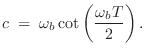
where
Thus, given a particular desired break-frequency
![]() , we can set
, we can set
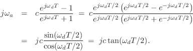
Recall from Eq.![]() (8.19) that the transfer function of the
first-order analog allpass filter is given by
(8.19) that the transfer function of the
first-order analog allpass filter is given by
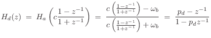
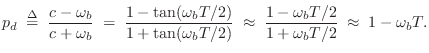
Figure 8.25 shows the digital phaser response curves corresponding
to the analog response curves in Fig.8.24. While the break
frequencies are preserved by construction, the notches have moved
slightly, although this is not visible from the plots. An overlay of
the total phase of the analog and digital allpass chains is shown in
Fig.8.26. We see that the phase responses of the analog and
digital alpass chains diverge visibly only above 9 kHz. The analog
phase response approaches zero in the limit as
![]() ,
while the digital phase response reaches zero at half the sampling
rate,
,
while the digital phase response reaches zero at half the sampling
rate, ![]() kHz in this case. This is a good example of when the
bilinear transform performs very well.
kHz in this case. This is a good example of when the
bilinear transform performs very well.
![\includegraphics[width=\twidth]{eps/phaser1d}](http://www.dsprelated.com/josimages_new/pasp/img1925.png) |
![\includegraphics[width=\twidth]{eps/phaser1ad}](http://www.dsprelated.com/josimages_new/pasp/img1926.png) |
In general, the bilinear transform works well to digitize feedforward analog structures in which the high-frequency warping is acceptable. When frequency warping is excessive, it can be alleviated by the use of oversampling; for example, the slight visible deviation in Fig.8.26 below 10 kHz can be largely eliminated by increasing the sampling rate by 15% or so. See the case of digitizing the Moog VCF for an example in which the presence of feedback in the analog circuit leads to a delay-free loop in the digitized system [479,477].
Next Section:
Phaser Notch Parameters
Previous Section:
Classic Analog Phase Shifters


