


Feedback Controllers - Making Hardware with Firmware. Part 8. Control Loop Test-bed
This part in the series will consider the signals, measurements, analyses and configurations for testing high-speed low-latency feedback loops and their controllers. Along with basic test signals, a versatile IFFT signal generation scheme will be discussed and implemented. A simple controller under test will be constructed to demonstrate the analysis principles in preparation for the design and evaluation of specific controllers and closed-loop applications.
Additional design notes will be published in due course, on the project website here and the latest developments can be followed on Twitter @precisiondsp. and LinkedIn- Part 8: Control Loop Test-bed (this part)
- Part 7: Turbo-charged Oscillators
- Part 6: Self-Calibration, Measurements and Signalling
- Part 5: Some FPGA Aspects
- Part 4: Engineering of Evaluation Hardware
- Part 3: Sampled Data Aspects
- Part 2: Ideal Model Examples
- Part 1: Introduction
As ever, it should be noted that any examples shown may not necessarily be the best or most complete solution.
***For some reason, the indented lists which are fine in the editor are not fine when published.***
Test-bed Aspects Considered in this Article
- Context & general development for the built-in Test-bed
- Summary of some key ADC/DAC specifications
- Measurements
- Signal Generation
- Signal generator - Test-bed signal types
- DC levels
- Single sine-waves, with and without "Turbo" sampling mode
- Arbitrary signal generation for control loop testing
- Ramp
- Pulses
- Step
- Inverse FFT (IFFT) signalling and motivation for control loop testing
- Test Configurations
- Open-loop controller testing
- Closed-loop application testing
- Self-Measurement of Practical IFFT Waveforms
- FFT analyses for Gain/Loss, Phase and Latency testing
- Discussion and Conclusions
1. Context & general development for the built-in Test-bed
This project is concerned with the development of high-speed low-latency controllers and an example closed-loop application that can make arbitrary (within reason) 1 and 2 port electrical/electronic circuits.
An evaluation unit has been designed and manufactured to evaluate what levels of functionality and performance can be achieved using modestly-priced and readily available technology with a particular emphasis on floating-point FPGA devices such as the Cyclone V and the emerging Cyclone 10 GX parts from Intel.
Given that the unit's 2-channel controllers/closed-loop circuits naturally incorporate ADC and DAC devices, it made sense to design in a small amount of additional flexibility to provide a Signals and Measurement Test-bed for the evaluation of the Controllers and Closed-loop applications.
As part of the general and test-bed development, the ADC, DAC and Signal Generation sampling rates have been increased and unified since the previous articles.
2. Summary of some key ADC/DAC specifications
a. Measurements
ADC Sample Rate - The 16 bit ADC sample rate has been increased from it's previous value of 4 Msps to a new value of 8 Msps (Nyquist = 4MHz). The maximum possible rate for the LinearTech/ADI LTC2387-16 device is 15 Msps. There is an option to fit an 18 bit pin compatible device.
ADC Noise Floor - Is around -120 dB(relative to full scale), as shown in the Fig 1 below.
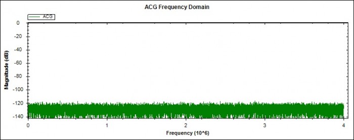
Fig 1. ADC Noise Floor - Measuring 0V reference.
b. Signal Generation
DAC Sample Rate - The 16 bit DAC sample rate is 24 Msps. The maximum possible rate for the LinearTech/ADI LTC1668 device is 50 Msps. The 24 Msps figure is a limitation due to the 2 main DACs and the 2 optional auxiliary DACs sharing a multiplexed data bus. Operation to 48 Msps is envisaged if the auxiliary DACs are not used or if only one channel is active.
3. Signal generator - Test-bed signal types
a. DC levels
DC signals are typically used for steady-state evaluation of controllers and closed-loop systems. High accuracy DC levels can be applied and measured by the Test-bed.
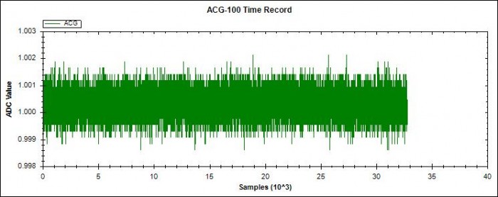
Fig 2. Application and measurement of 1V DC test signal.
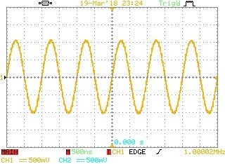
b. Single sine-waves, with and without "Turbo" sampling mode
Sine-wave testing is a standard method for evaluating the Magnitude and Phase performance of controllers and closed-loop applications. Some applications are envisaged that will make use of an alternative result presentation, using the Real and Imaginary components of the measured signals rather than Magnitude and Phase.
Single frequency sine-waves are provided by a floating-point "Biquad Oscillator which operates at 8Msps. This maximum Biquad speed is limited by FPGA latency. A "Turbo" arrangement described in the previous Blog extends the sampling rate to 24Msps. The Cyclone 10 GX future option offers a much lower floating point latency which will not require the "Turbo" mode in this application, but may well do in other higher frequency applications.
Here are some wave-forms generated by the floating-point sine-wave oscillator
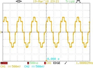
Fig 3. A 1MHz Biquad Sine-wave at Max FPGA floating-point rate due to FPGA Cycle latency.
c. Arbitrary signal generation for control loop testing
An arbitrary signal generator has been implemented that is currently set for a 32k samples record, 24Msps sample rate and a 16 bit resolution. The record can be continuously repeated. Some of the initial wave-forms are :-
i. Ramp - The Ramp waveform is another well-known signal used for evaluation how well feedback control systems can follow a simple moving demand signal. The following is an example Ramp generated by the arbitrary signal generator.
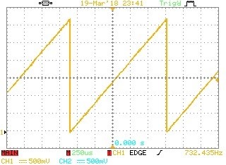
Fig 5. Ramp test waveform from the arbitrary signal generator.
ii. Pulses - another standard control system test signal
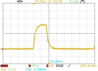
Fig 6. A single sample pulse of 41.67ns. The rise/fall-time is due to scope and probe.
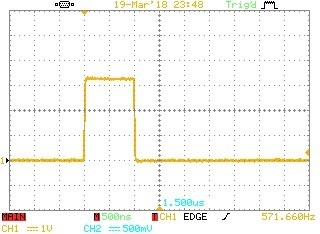
Fig 7. This is another example pulse, this time it has a duration of 1us.
iii. Step - another standard control system test signal
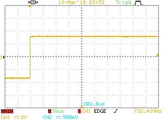
Fig 8. Step test waveform from the arbitrary signal generator.
iv. Inverse FFT (IFFT) signalling and motivation for control loop testing
There are a variety graphing methods for assessing control loop characteristics. Principle among these are the Bode, Nyquist & Nichols Charts. They present in various ways the transfer function or output/input characteristic of the block being designed/evaluated. In each case the output/input relationship is determined at a number of frequencies and then plotted over the frequency range of interest. In some cases the output/input is expressed as Magnitude and Phase and in other cases Real and Imaginary components.
For the sake of efficiency, it would be nice to test at more than one frequency at a time.
So, having spent a fair amount of time creating a single sine-wave generator, we are now going to look a block that can produce 16,384 sine-waves + an optional dc level, at the same time.
Whereas the well-known FFT algorithm takes sequence data (typically a time sequence) and transforms it into frequency domain data, the IFFT provides the inverse operation to give sequence data from frequency domain data. In the general case FFT and IFFT inputs and outputs might both be complex and might also be multi-dimensional vectors.
In this discussion, the IFFT input will be limited to a single array of complex frequency domain data and the IFFT output will be a single array of time sequence point values which are loaded into the arbitrary signal generator RAM store.
There are plenty of resources on this site and elsewhere that discuss FFTs, etc. but here are just a few points to note, especially in the use of IFFTs.
- Different implementations of an IFFT may use different scaling factors or have options for input and/or output scaling factors.
- Different IFFT implementations may use differing layouts for the frequency domain information e.g.where the d.c., Nyquist, +ve and -ve frequency array locations (sometimes called bins) are placed.
- In some cases FFT/IFFT operations may omit -ve frequencies and include their contribution within the +ve frequency components.
- Creating simple test cases will show what is going on and allow confirmation of scaling, +ve and -ve frequency use and array layout.
In the examples that follow, I will use the MATLAB IFFT for general examples and the Math.NET Numerics
void Inverse(Double[] real, Double[] imaginary, FourierOptions options), for the evaluation hardware.
For a 1st set of MATLAB exercises, we will look at using the IFFT to Generate various signals from an array of 16 frequency domain values. We will start with using a single Real array. The Array allocations for the IFFT input are :-
| dc, | +F1, |
+F2, |
+F3, |
+F4, |
+F5, |
+F6, | +F7, | FNyq, | -F7, | -F6, | -F5, | -F4, | -F3, | -F2, |
-F1 |
Where dc is the dc component, F1 to F7 are 7 frequencies in ascending order and FNyq is the Nyquist frequency = Sampling Rate/2.
Here are some example IFFT output sequences for a variety of frequency array settings. In the present context, these will be the time wave-forms generated by the arbitrary signal generator.
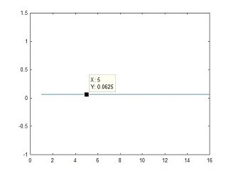
Fig 9. dc level only at array location "dc"
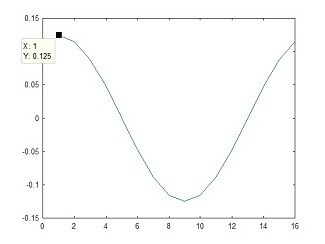
Fig 10. a single sine-wave at locations +F1,-F1
X = [1,0,0,0,0,0,0,0,0,0,0,0,0,0,0,0]; % Set a dc level only
Z= ifft(X);                            % perform the Inverse FFT
plot(Z)                                % Show the resulting sequence
Code for Fig 9.
X = [0,1,0,0,0,0,0,0,0,0,0,0,0,0,0,1]; % Set a low frequency sinewave
Z= ifft(X);                            % perform the Inverse FFT
plot(Z)                                % Show the resulting sequence
Code for Fig 10.
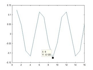
Fig 11. a single sine-wave at locations +F3,-F3
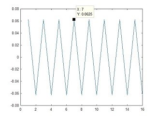
Fig 12. a single sine-wave at location "FNyq"
X = [0,0,0,1,0,0,0,0,0,0,0,0,0,1,0,0]; % Set a mid freq sinewave
Z= ifft(X);                            % perform the Inverse FFT
plot(Z)                                % Show the resulting sequence
Code for Fig 11.
X = [0,0,0,0,0,0,0,0,1,0,0,0,0,0,0,0]; % Set a sinewave at Nyquist
Z= ifft(X);                            % perform the Inverse FFT
plot(Z)                                % Show the resulting sequence
Code for Fig 12.
Notes
- To keep the IFFT output real, the frequency domain information for all frequencies other than dc and FNyq must be provided in equal Real pairs ( and later, in complex conjugate pairs).
- We can see what amplitude sine-waves/scaling factor you get from entering 1's in the frequency domain.
- We see that we get twice the amplitude contribution from the +/- pairs compared with the single FNyq array entry.
- All the sine-waves are complete cycles meaning that we can continuously repeat the sequence and not suffer any discontinuities. Also if we collect measurements at a multiple of the transmitted sequence, then we do not need to window the records.
and now ..
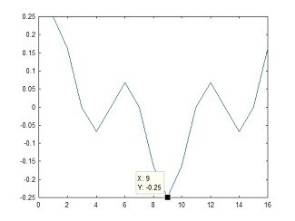
Fig 13. Multiple sine-waves
X = [0,1,0,1,0,0,0,0,0,0,0,0,0,1,0,1]; % Multiple sinewaves
Z= ifft(X);                            % perform the Inverse FFT
plot(Z)                                % Show the resulting sequence
Code for Fig 13.
Generating a flat spectrum, Plan A and Plan B
Now we can look at generating a broad spectrum of sine-waves for use in Bode Plotting etc.
The following plots show the frequency spectra resulting from 2 completely different test wave-forms.
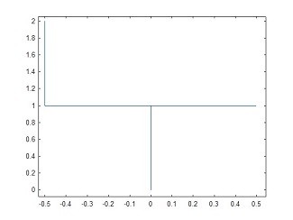
Fig 14. Flat spectral response, Plan A
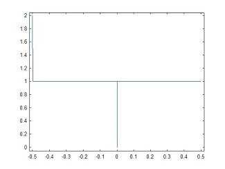
Fig 15. Flat spectral response, Plan B
Apologies for the switch in bin ordering for the FFT display, which is now :- FNyq shown at the left hand edge, then -ve frequencies, then the dc level and finally the +ve frequencies. For simple plotting it's either this or showing the -ve frequencies in the range 0.5 -> 1.0 which is even stranger.
OK, remembering to add the +ve and -ve magnitudes together, we have an effective magnitude from > dc to FNyquist = 2.0 across the whole band.
Now to the time domain signals that produced these identical frequency responses.
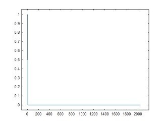
Fig 16. Flat spectral response, Plan A
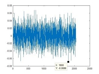
Fig 17. Flat spectral response, Plan B
The key message from this is that if you want to get a flat spectrum of test frequencies, you can either provide the "Random" noise signal generated by the IFFT in Plan B or you can apply an impulse with a magnitude some 1/0.0686 = 14.6 times higher as shown in Plan A.
In a practical system we would prefer to apply a test signal of say +-5 volts based on Plan B than a single pulse of 14.6 * 5 = 73 volts based on Plan A, to get the same effect.
The code for both Plan A and Plan B follows. The only difference is that the sine-waves in Plan A all have the same phase and the sine-waves in Plan B each have a "Random" phase.
dc = 0 ;           % Set the dc value = 0
PosF =  ones(1,1023); % Create an array 7 +ve frequencies, level = 1
FNyq = 2.0 ;       % Set the Nyquist Frequency at Level = 2.0
NegF = flip(PosF); % Create the reflected array of -ve frequency entries
FArray = horzcat(dc,PosF,FNyq,NegF); %Build the sections into an array
SeqArray = ifft(FArray);             % Perform the Inverse FFT
plot(SeqArray)                       % Show the resulting sequence
n = length(SeqArray);
X = fft(SeqArray);    % Now convert back to the frequency domain
Y = fftshift(X);      % Shift the Sequence Array format for display
fshift = (-n/2:n/2-1)*(1/n); % Create frequency axis values
mag = abs(Y);           % Convert complex to magnitude
plot(fshift,mag)        % Show the Frequency domain plot
Code for Fig 16, Plan A
dc = complex(0.0,0.0) ;           % Set the dc to Real level = 0.0
                   % Now create an array of "Random" Phase sinewaves
Ph = 2*pi*rand(1,1023); % Make 1023 "Random" Phase values between 0->2*Pi
Mag =  ones(1,1023);    % Make 1023 Magnitude = 1 values
[BinRe,BinIm] = pol2cart(Ph,Mag); % Convert Magnitude & Phase to Re, Im
PosF = complex(BinRe,BinIm);      % Create +ve Frequency Array
FNyq = complex(2.0,0.0) ;         % Nyquist Frequency is Real level = 2.0
PosFConj = conj(PosF);            % Make the complex conjugate of PosF
NegF = flip(PosFConj); %Create the reflected array of -ve frequency entries
FArray = horzcat(dc,PosF,FNyq,NegF); %Build the sections into an array
SeqArray = ifft(FArray);             % Perform the Inverse FFT
plot(SeqArray)                       % Show the resulting sequence
n = length(SeqArray);
X = fft(SeqArray);    % Now convert back to the frequency domain
Y = fftshift(X);      % Shift the Sequence Array format for display
fshift = (-n/2:n/2-1)*(1/n); % Create frequency axis values
mag = abs(Y);           % convert to magnitude
plot(fshift,mag)        % Show the Frequency domain plot
Code for Fig 17, Plan B
4. Test Configurations
Each of the two Channels in the evaluation unit can be configured in a variety of ways. These include :-
- as a controller with 1 input port and 1 output port
- as a single Input/Output port to provide the closed-loop circuit emulation application
- as a 1 or 2 port test and measurement unit with signal generation and measurement either combined in 1 port or separated to 2 ports. Additional, a variety of signal load and feed options are available.
The signal generation and measurements blocks can be fully synchronized to guarantee that stimulus and measurements are precisely linked.
a. Open-loop controller testing - voltage out/voltage in
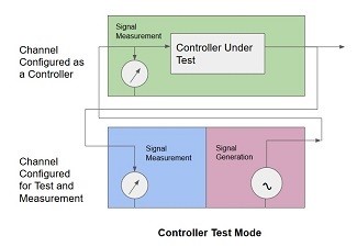
Fig 18. Option 1 for Output/Input Testing
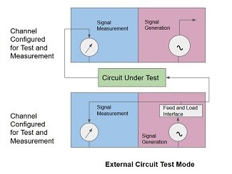
Fig 19. Option 2 for Output/Input Testing
b. Closed-loop application testing - port voltage/port current
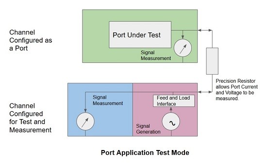
Fig 20. One of the possibilities for measuring I/O Port Characteristics
5. Self-Measurement of Practical IFFT Waveforms
A Selection of Test Signals generated by the IFFT/Arbitrary Signal Generator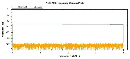
Fig 21. The Green Channel 1 Plot shows an IFFT / Arbitrary Signal
Generator waveform where all of the frequency bins are active except for
dc and Nyquist. The Orange plot is the Channel 2 noise floor.
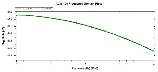
Fig 22.This plot shows the detail of the spectral signal. There is
around a 1 dB drop from dc to Nyquist due to the ADC filtering. In any
case many of the tests will be ratio based so the exact flatness is not
important. For other tests a simple 1st order digital filter will
provide correction.
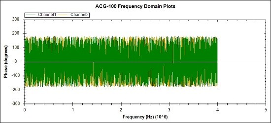
Fig 23. The Green plot shows the phase of the IFFT based "Random" signal
on Channel 1 and the Orange plot shows the phase of the random noise
floor signal on Channel 2.
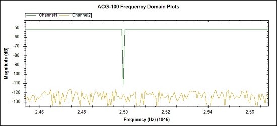
Fig 24. In this case a single frequency bin at 2.5MHz has been turned
off to demonstrate a "missing bin" test. This type of test is used to
prove that no undue distortion from hardware or mathematical sources is
present, that would result in inter-bin corruption.The missing bin is
clean down to -111 dB.
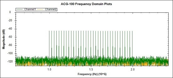
Fig 25. Finally an image showing that only part of the spectrum can be
selected and that bins can be skipped. This case might be used to allow a
smaller number of stronger signals to be used to probe specific
portions of the frequency band.
6. FFT analyses for Gain/Loss, Phase and Latency testing
Now that we have methods for multiple sine-wave generation, signal capture and configurations for 2-port testing, we can look at setting up and analyzing signals for Bode Plots and the like. In addition to the standard Magnitude and Phase measurements a simple extension to provide a Latency calculation will also be added. In this context the Latency between the input and output signals is defined as :-
Latency(f) = Phase difference input to output in degrees / (360 * f) ... for each frequency f tested.
Results for an uncalibrated divider network
A test circuit was constructed to provide an initial check on the methods and analysis.
The schematic is :-
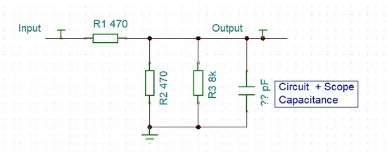
Fig 26. A Test Circuit made with 1% resistors and unknown capacitance.
The calculation for loss at dc is -6.27 dB
Fig 27. This is the test waveform applied to the test network of Fig 26.
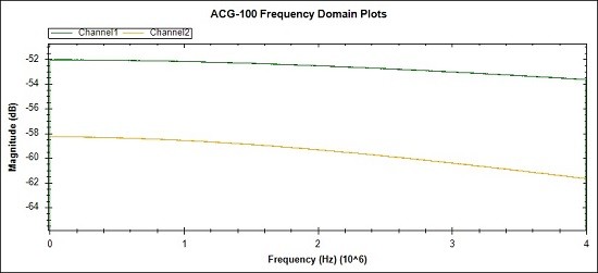
Fig 28. These are the frequency domain magnitude measurements of the
test network input signal (Green trace) and the corresponding output
signal (Orange trace).
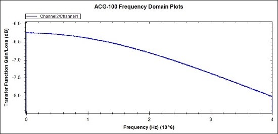
Fig 29. This plot shows the output/input frequency response of the network under test.
The loss at 1MHz is -6.38 dB
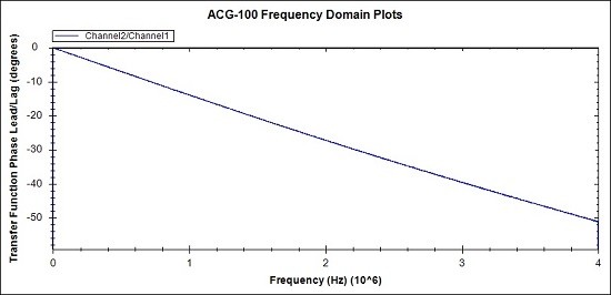
Fig 30. This plot is the phase lag produced by the network under test.
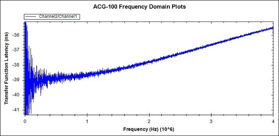
Fig 31. This latency plot is derived from the phase plot above and the
frequency corresponding to each phase point. The Latency at 1MHz is
38.6ns.
Rough Confirming Measurements
Oscilloscope measurements were made to provide a rough confirmation of the above results at 1MHz.
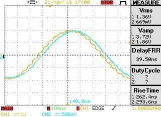
Fig 32. Rough confirming scope reports for 1MHz.
Scope plots of a 1MHz signal from the floating-point signal generator to the test network input (yellow trace) and the output signal resulting (blue trace).
1MHz signal loss is calculated as 20*Log10 (669/1360) = -6.16 dB
The Delay/Latency is reported as = 39.5 ns
Note -The Scope Vrms and Delay reporting are rather noisy and could benefit from an averaging exercise.
In Summary :-
| Measurement Type | ACG-100 IFFT/FFT Analysis |
Ideal Calculation |
Rough Scope Measurement | Difference |
|---|---|---|---|---|
| DC Loss | -6.25 dB |
-6.27 dB | 0.02 dB |
|
| 1MHz Loss |
-6.38 dB | -6.16 dB (noisy) | -0.22 dB | |
| 1MHz Latency | 38.6 ns. | 39.5 ns (noisy) | -0.9 ns |
Table 1. Summary of measurements and confirming results.
Further due diligence is required, but the 1st impressions are most promising.
7. Discussion and Conclusions
The developments for this stage of the project included the FPGA activities of upgrading the ADC and DAC sample rates, ensuring close synchronization for all generated and measured signals, incorporating the "Turbo" sine-wave scheme previously described, developing the arbitrary signal generator and upgrading the FPGA/PC command and control interface.
The PC user interface required C# updates to manage the new signal generator controls, generate the IFFT signals, pass the arbitrary wave-forms to the FPGA, provide FFT and associated analysis and present the results to screen.
On the science side the extensions were to bring IFFT and FFT techniques used on previous projects into the current project.
Out of all that activity, the toughest part was working at nano-second and sub nano-second timing in the management by the FPGA of the ADC and the DAC Multiplex system. Although the ADC and DAC sample rates are modest, the clocks and timings associated with them are running at several hundred MHz.
The next phase of the project will see the FPGA implementation of Controller Transfer Functions for the 1st time on the evaluation unit.
Conclusions
The IFFT and associated FFT analysis along with the hardware, firmware and software that run them have added a powerful diagnostic and self-diagnostic capability to the evaluation unit. The expectation is that the performance of controllers along with associated open-loop and closed loop applications can now be developed and tested with accurate measurements for signal levels, phase and latency.
Thank you for your interest, Steve Twitter @precisiondsp. and LinkedIn
Next up will be - Some initial results for controllers and closed-loop application.
- Comments
- Write a Comment Select to add a comment
To post reply to a comment, click on the 'reply' button attached to each comment. To post a new comment (not a reply to a comment) check out the 'Write a Comment' tab at the top of the comments.
Please login (on the right) if you already have an account on this platform.
Otherwise, please use this form to register (free) an join one of the largest online community for Electrical/Embedded/DSP/FPGA/ML engineers:


