


Feedback Controllers - Making Hardware with Firmware. Part 7. Turbo-charged DSP Oscillators
Comparisons will be made between implementations on Intel Cyclone V and Cyclone 10 GX FPGAs. An Intel numerically controlled oscillator (NCO) IP block will also be considered.
Additional design notes will be published
in due course, on the project website here and the latest developments can be followed on Twitter @precisiondsp. and LinkedIn
- Part 7: Turbo-charged Oscillators (This Part)
- Part 6: Self-Calibration, Measurements and Signalling
- Part 5: Some FPGA Aspects
- Part 4: Engineering of Evaluation Hardware
- Part 3: Sampled Data Aspects
- Part 2: Ideal Model Examples
- Part 1: Introduction
As ever, it should be noted that any examples shown may not necessarily be the best or most complete solution.
Oscillator Aspects Considered in this Article
- Context for the Oscillator requirements
- Some DSP Oscillators for evaluation
a. Intel Numerically Controlled Oscillator (NCO) IP - Multiplier Option
b. Floating-Point Recursive - Biquad on Cyclone V
c. Floating-Point Recursive - Boosted Sample Rate on Cyclone V
d. Floating-Point Recursive - Biquad on Cyclone 10 GX - Oscillator Implementation Comparisons
- Spectral purity
- Amplitude stability
- Resources
- Cost
- Discussion and Conclusions
1. Context for the Oscillator requirements
One of the objectives for this project is to see what can be achieved with floating-point centric FPGAs. So, we will continue with that focus for signal arithmetic unless circumstances dictate a need for a fixed-point solution.
In terms of functionality, this project will require the generation of DC, Sine-wave, Square-wave, Noise and Arbitrary-wave signals. This article will concentrate on the Sine-wave ( + Bonus Square-wave) generation.
The Sine-wave Oscillators discussed here will be simple and/or easy to implement, but the project may well end up with more complex designs.
The ADI/LinearTech 16 bit DAC's have a maximum sample rate of 50Msps. The oscillator designs discussed here which drive those DACs will be be aimed for a sample-rate of 48Msps.
2. Some DSP Oscillators for evaluation
For some general background reading on DSP oscillators. I have found the following useful.
Phillips - Algorithms and architectures.... Chapter 7.
...and now a look at some specific FPGA implementations
a. Intel Numerically Controlled Oscillator (NCO) IP - Multiplier Option
The Intel NCO component is one of the IP components provided with the Quartus Prime FPGA development suite and is documented here. It is a commercial package which offers a wide variety of implementation options whereby
you can typically trade FPGA resource types and complexity against level
of performance. It is free to evaluate but requires a license for use in a distributable application.
According to Mouser, the cost of the Intel NCO IP is $2,502.49
The Intel NCO arrangement is shown in the following diagram.
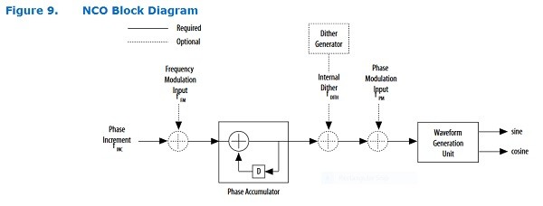
Fig 1. Illustration of the NCO from the Quartus IP Document
and a description of the trade-offs for the various architecture options.
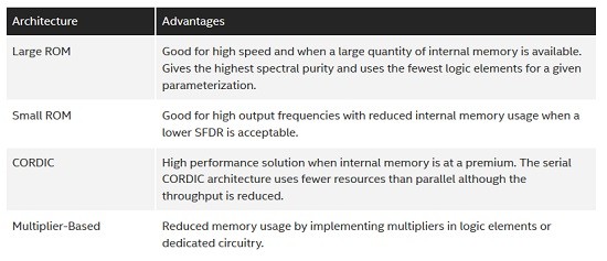
Fig 2. NCO architecture comparison from the Quartus IP Document
One nice feature of the Quartus IP configuration utility is that it provides a spectral plot of oscillator performance as you play with the configuration settings enabling comparisons to be made without actually needing to build or compile any designs. e.g.
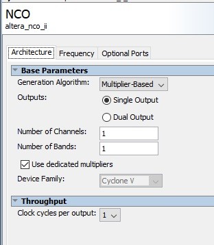
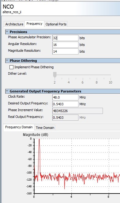
Fig 3. Predicted Oscillator Spectral Performance for a Cyclone V Hardened Multiplier Design
The FPGA resources needed for an unspecified Oscillator are illustrated as follows :-
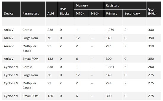
Fig 4. Typical FPGA Resources required.
Based on comparing resources and performance, the Multiplier-Based configuration was chosen for the Cyclone V FPGA. With 1 sample produced on each clock cycle and an fmax of 275 MHz, there is no problem in meeting our target of 48Msps if we use a 48MHz clock.
The Multiplier-based Oscillator produced the following spectral plot from the unit ADC measurements.
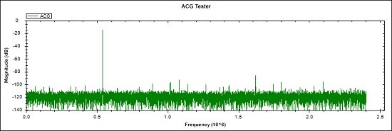
Fig 5. Self-measured spectral response for the Intel NCO IP Oscillator, Multiplier Configuration
Notes for Fig 5.
- NCO signal = -14.3dB at 540.3KHz, Largest spurious component -86dB at 1.62085MHz
- Fig 5. is a measurement made by the unit ADC of the NCO signal from FPGA via a DAC, DAC op amps, Port amplifier, Port sampling divider + op amp and the ADC driver.
- NCO fixed amplitude bits = 14 ( to provide a mid-range ADC signal )
- NCO sample rate = 48Msps
- ADC Sampling Rate = 4.8Msps (to be increased later)
- FFT is 32768 time samples with a Blackman-Harris Window
- 0 dB is ADC full-scale
- Spurious-free (SFDR) range is 71.7dB with no dither applied. (Dither to improve SFDR is available)
- A practical design using the Intel NCO IP would require additional amplitude control blocks
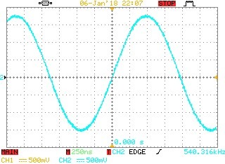
... and the physical o/p signal
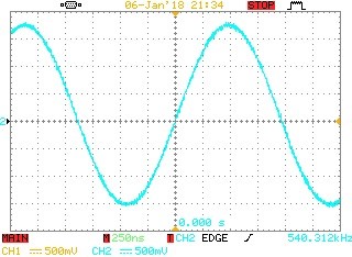
Measurement made with a limited resolution oscilloscope and non-ideal probe earthing.
Fig 6. Intel NCO IP waveform at the unit Port o/p
b. Floating-Point Recursive - Biquad on Cyclone V
The simple Biquad recursive design is illustrated as :-
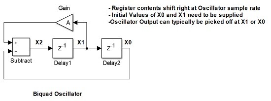
Fig 7. Basic Recursive Biquad Oscillator
which is described by the equation $X2(n) = A*X1(n) - X0(n) $
or alternatively the recursive equation $X2(n) = A*X2(n-1) - X2(n-2) $
and $A = 2*Cos(Fosc*2*Pi*Ts)$
where $Fosc$ is the desired oscillator frequency and $Ts$ is the sample period
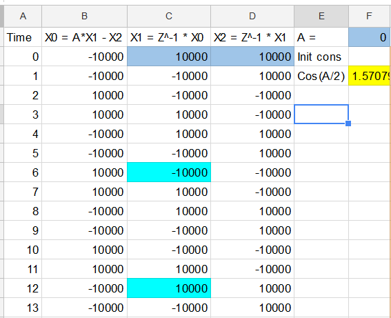
We can make one of these on a spreadsheet as shown next. Note that the Google spreadsheet precision is undoubtedly higher than the planned FPGA single precision format.
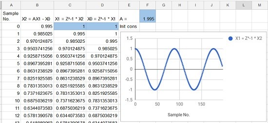
Fig 8. Basic Recursive Biquad Oscillator - Spreadsheet version
where $A=1.995, X0(0) = 1$ and $X1(0) = 1$ and the o/p is $X1$ which is graphed.
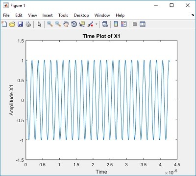
and here is a MATLAB single-precision version plot
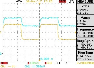
Biquad Squarewave bonus
If we set the frequency determining value A = 0, we get a square wave.
 ddd
ddd
Fig 10. Example square wave generated by a Biquad with A = 0.
The yellow trace is the signal as it appears on the unit SMA port connector.
Risetime in part due to scope and scope probe.
The arrangement of Fig 7. was implemented for the Cyclone V using the Quartus ALTERA_FP_FUNCTIONS which are documented here.
Problem
The Cyclone V floating-point blocks can be tuned for a balance between operating frequency and cycle latency but the actual time latency is a minimum at around 50MHz and 2 Cycles for both multiply and subtract blocks. This latency is important because we can't get the next value in the oscillator sequence until the multiply and subtract are done. For a variety of reasons, the Biquad oscillator was run at 48MHz with 6 Cycles between generated samples i.e. an oscillator sample rate of 8Msps which falls well short of our 48Msps requirement.
The resulting highly quantized 540.3KHz waveform is shown immediately below
 Simple floating-point oscillator
 Intel NCO IP Oscillator
Fig 11. Basic floating-point recursive waveform compared with the Intel NCO IP, Multiplier option
The Cyclone V cannot meet the 48Msps requirement with a simple recursive oscillator. Options are :-
- Go with the Commercial NCO and add some amplitude control blocks, but that is expensive at this stage and not our desired floating-point solution.
- Find or develop an alternative NCO. That would require unknown time and effort and is also not likely to be a floating-point solution
- Devise an alternative floating-point based solution. OK, let's do that.
c. Floating-Point Recursive - Boosted Sample Rate on Cyclone V
Plan A - Run multiple oscillators at different phases and combine them.
Problem - Even when set to the same frequency, multiple recursive oscillators can exhibit small actual frequency differences when they are each set to a different initial condition. This was not analyzed but is most likely due to arithmetic quantization.
Plan B - Run a modified recursive oscillator at 48Msps in an arrangement like this ..
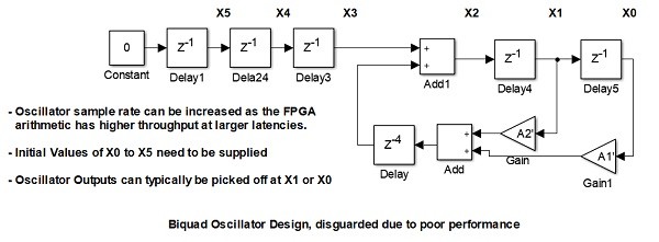
Fig 12. Plan B. Accounting for the calculation latency
Here, we must modify the calculation for X2 so that the correct values appear when they become available after the unavoidable calculation delay. In the interim, pre-calculated values must be fed into X2 until the "live" calculations start appearing.
Plan C - Run a recursive oscillator at 8Msps and calculate fill-in values from the slow oscillator values to construct a 48Msps waveform in an arrangement like this ...
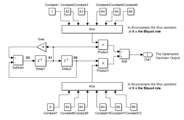
Fig 13. Plan C. Calculating a small but fast sequence of waveform points from a slow recursive oscillator
We thus have a slow Biquad providing samples at 8Msps. and for example a 6 position Mux running at 6 * 8 = 48Msps which produces the 6 waveform values needed until the next Biquad values are available.
The detail is beyond this blog, but the spreadsheet version looks like this..
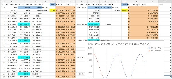
Fig 14. Spreadsheet for the augmented slow recursive oscillator
The desired 48Msps values are in column C, The "slow" 8Msps oscillator values are in every 6th row in columns I, J & K. The 12 constants needed to generate the high sample rate values from the slow sample rate values are in orange in columns N & O and finally the high sample rate values are generated by applying the 12 constants to the slow sample rate values in column J which is the oscillator output.
The FPGA implementation looks like this ...
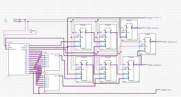
Fig 15. FPGA implementation for the augmented slow recursive oscillator
Again, this is not intended to show detail and in any case it is not optimized, but in rough terms it consists of :-
- A "slow" biquad oscillator consisting of a multiplier, a subtractor, a floating-point to fixed-point convertor (for debug purposes)and management of the signal registers.
- An upsampling calculator consisting of 2 multipliers, 2 Multiplexers, a summer, 12 Constant values, a floating-point to fixed-point convertor and management of the Multiplexers in synch with the Oscillator.
The results from this are ...
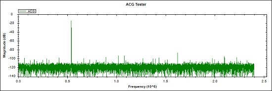
Fig 16. Self-measured spectral response for the augmented floating-point recursive oscillator
Notes for Fig 16.
- Augmented Biquad signal = -14.3dB at 540.3KHz, Largest spurious component -86.7dB at 1.62085MHz
- Spurious-free (SFDR) range is improved to 72.4dB compared to the Intel NCO IP of 71.7dB
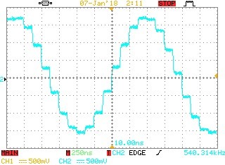
Measurement made with a limited resolution oscilloscope and non-ideal probe earthing.
Fig 17. Augmented Biquad oscillator waveform at the unit Port o/p
d. Floating-Point Recursive - Biquad on Cyclone 10 GX
For our final oscillator we will go back to the simple Biquad recursive scheme, but this time it will be implemented on the Cyclone 10 GX FPGA which is the latest Cyclone offering from Intel.
This exercise is limited to compilations and simulations as I don't yet have a physical Cyclone 10 GX dev. kit to attach to the unit mixed-signal circuits.
This time it's a really simple FPGA implementation ...
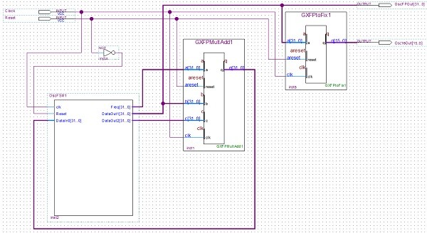
Fig 18. A Cyclone 10 GX recursive oscillator
The Cyclone 10 GX IP library includes a Multiply then Add block. This together with a floating-point conversion and some simple register control logic make the complete oscillator.
Notes for the Cyclone 10 GX recursive oscillator are :-
- Multiply/Add Latency is 4 Cycles, so allow 5 Clock cycles per Oscillator sample.
- Required Oscillator sample rate = 48Msps
- Clock = 48Msps * 5 = 240MHz
- Because we actually want a Multiply then Subtract, we flip the sign bit of the data supplied to the Add port.
- Worst case clock rate for the slowest Cyclone 10 GX part Multiply then Add is 270MHz, so a 240MHz clock frequency is fine.
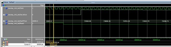
The simulated results are :-
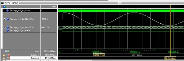
Fig 19. Simulated Cyclone 10 GX recursive oscillator producing a 540.3kHz Sine-wave
3. Oscillator Implementation Comparisons
| Oscillator Type | Spectral Purity of DAC/ADC Chain | Amplitude Stability | Approx Resources | Cost |
|---|---|---|---|---|
| Intel NCO IP Cyclone V | SFDR 71.7dB | NCO is inherently stable | 92 ALMs 2 DSP Blocks 2 M10 Mem blocks 246 Registers | $2,502.49 |
| Floating Point Biquad Cyclone V | Could not achieve 48Msps | untested | Don't Care, it's not a contender | Small time and effort |
| Boosted Floating Point Biquad Cyclone V | SFDR 72.4dB | within +-0.002% Vrms readings over 1 hour | 996 ALMs 3 DSP Blocks 0 M10 Mem blocks 577 Registers | Significant time and effort |
| Floating Point Biquad Cyclone 10 GX | Anticipate same as above | Anticipate same as above | 92 ALMs 1 DSP Blocks 0 M10 Mem blocks 197 Registers | Small time and effort |
| New Design NCO Cyclone V | ??? | Inherently stable | ??? | ??? |
Table 1. Comparison of Oscillator types
4. Discussion and Conclusions
Intel NCO IP - For some projects, the Intel NCO type oscillator is a no-brainer as it is flexible, scalable, efficient, guaranteed stable, performs well and is supported across the Intel FPGA range. For some companies the cost of the IP can be justified by the ease of design and implementation that a commercial package offers. Of course, if a competent lower-cost alternative were available that offered similar features, then that would be even more attractive.
As far as I can tell, the Intel NCO IP is a fixed amplitude oscillator which can be set at the desired No of Bits. so, if variable amplitude were needed on the digital signal, then that would require additional blocks.
Floating-point recursive oscillators - My fixation on floating-point recursive oscillators derives from the joy some years ago of being able to create a high-quality sine wave oscillator on a Sharc DSP with just a few lines of c code.
Recursive oscillators are not guaranteed to be amplitude stable, due to imperfect arithmetic precision but for my present applications and using single-precision arithmetic, an observed stability of within +-0.002% Vrms readings over 1 hour is more than good enough (Although that was only at one frequency and one set of initial conditions).
The amplitude and phase of the recursive Biquad can be controlled by setting the initial state values.
But, the Cyclone V cannot run a simple floating-point Biquad quickly enough to attain a 48Msps sample rate although that could be seen as an unnecessary challenge in creating a sine-wave oscillator.
"Turbo-charged" recursive oscillator (Cyclone V) - The arrangement described to provide an n times increase in floating-point sample rate over the basic recursive oscillator works well. It does not add any further concerns for stability and in the context of the Mixed-Signal circuitry, it provides an equal performance to the Intel NCO IP. Significantly greater general FPGA resources are required over the NCO IP due to the floating-point operation of the recursive oscillator but at < 1% of the ALMs and DSP blocks available, that's not yet a concern.
Floating-point recursive oscillator(Cyclone 10 GX) - In theory this is just about the simplest and lowest FPGA resource floating-point oscillator on offer, with non-optimized FPGA resources as follows.
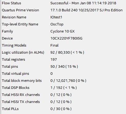
Fig 21. Cyclone 10 GX FPGA Recursive Oscillator Resources Needed (non-optimized).
In this application, the Cyclone 10 GX provides a performance 6 x greater than the Cyclone V ( with no optimizations considered) , so the fact that the Cyclone 10 GX offers 192 DSP blocks compared to 342 DSP blocks in the Cyclone V is likely to be more than compensated by the speed and efficiency gains.
Conclusions
For this project, right now, on the Cyclone V FPGA, the augmented Biquad recursive oscillator offers the required performance and the FPGA resources needed for it are fine at the moment. There has been a cost in time and effort to develop the design process and implement a working FPGA block, but the gain in knowledge was worth it. The cost of the commercial NCO IP cannot be justified at this stage.
It could be that a lower-cost non-recursive NCO could be found or designed and that remains an option for the future.
The Cyclone 10 GX theoretical design and simulation indicate that great strides are being made in the "number-crunching" capability being offered at the "economy" end of FPGA offerings.
Thank you for your interest, Steve Twitter @precisiondsp. and LinkedIn
Next up will be - Open and Closed-Loop Test Methods- Comments
- Write a Comment Select to add a comment

Hi Steve. Wow. Your comprehensive blog is rich in technical details! I have no experience with FPGAs so I hope you'll tolerate my "dumb" questions:
[1] I was startled by the graphical notation for the biquad in your Figure 7. It looks like a rectangle containing the letter 'A' means "multiply by A", and the circular multiply symbol actually means "addition." Is that graphical notation standard (traditional) in the discipline of FPGAs?
[2] I modeled your Figure 7 biquad with MATLAB (both fixed-pont and floating point art. Assuming my MATLAB code is correct (not always a safe assumption!), when I set A = 0 the output sequence was an Fs/4 Hz triangular sequence. When I set A = 1 the output sequence was an Fs/6 Hz squarewave-like sequence. I wonder if my modeling is incorrect.
[3] In your Figure 13, does a rectangle containing the letter 'X' mean "linear interpolation"?
[4] Does the label "O/P" mean "output"?
Thanks!

Hi Rick, Thank you for the comments. I'm sure none of your points are "dumb". I'll get to your points a bit later and I suspect that I might need to sharpen up the notations a bit when I work out which hat I've got on and whether I should use i or j.
Hi Rick,
[1] I was startled by the graphical notation for the biquad in your Figure 7. It looks like a rectangle containing the letter 'A' means "multiply by A", and the circular multiply symbol actually means "addition." Is that graphical notation standard (traditional) in the discipline of FPGAs?
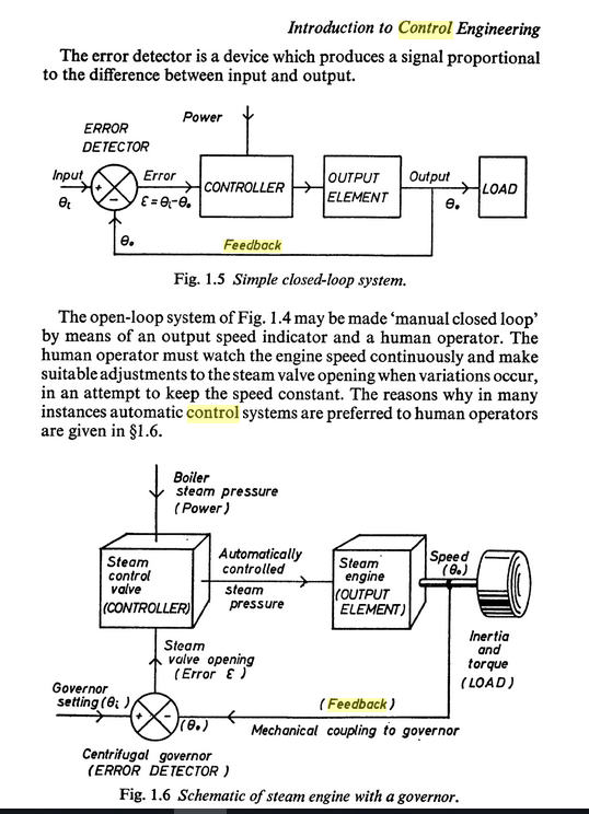
Ha, That is because I learned Feedback Control Systems in the 70's, but still in use by the American Society of Mechanical Engineers in 2015 as below.

As you say, in this context the box is multiply, times, x, X, *,, or . depending on how I feel and the circle with an X is a traditional(old) symbol for summation, with a negative sign on the signal if it's to be subtracted.
[2] I modeled your Figure 7 biquad with MATLAB (both fixed-pont and floating point art. Assuming my MATLAB code is correct (not always a safe assumption!), when I set A = 0 the output sequence was an Fs/4 Hz triangular sequence. When I set A = 1 the output sequence was an Fs/6 Hz squarewave-like sequence. I wonder if my modeling is incorrect.
Here is my spreadsheet Biquad with A=0
[3] In your Figure 13, does a rectangle containing the letter 'X' mean "linear interpolation"?
It's just a simple 2 input, 1 output multiply
[4] Does the label "O/P" mean "output"?
Yes, indeed.
Thanks for those points, I'll tighten up the consistency and add some definitions in a while.
Hi Steve. Ah, now I see. Our differing outputs for A=0 are caused by your and my different initial conditions. Based on your initial conditions, A=0 does indeed produce a squarewave-like output. All is well.
By the way, in your Jan. 11 reply giving your Biquad spreadsheet with A=0, the spreadsheets 'X2' column seems to be a delayed version of the 'X1' column. But that relationship seems to contradict the delay line notation in your blog's Figure 7 where 'X0' a delayed version of 'X1'.
Regarding the following graphical symbol

meaning "addition" (or "subtraction"), that astounds me. I wonder how that convention got started. Doesn't that convention cause problems when electrical and mechanical engineers look at each other's drawings (schematics)?
Hi Rick, Yes, I originally started with one set of labeling and changed it for the Blog because it felt better. Then I skipped back to the old sheet with the old labeling for the reply.
Description from one of my undergraduate textbooks
"The purpose of this work is to provide a course of study in elementary
control theory which is self-contained and suitable for students of all
branches of engineering and of applied physics."
To post reply to a comment, click on the 'reply' button attached to each comment. To post a new comment (not a reply to a comment) check out the 'Write a Comment' tab at the top of the comments.
Please login (on the right) if you already have an account on this platform.
Otherwise, please use this form to register (free) an join one of the largest online community for Electrical/Embedded/DSP/FPGA/ML engineers:


