


Feedback Controllers - Making Hardware with Firmware. Part 6. Self-Calibration Related.
This article will consider the engineering of a self-calibration & self-test capability to enable the project hardware to be configured and its basic performance evaluated and verified, ready for the development of the low-latency controller DSP firmware and closed-loop applications. Performance specifications will be documented in due course, on the project website here.
- Part 6: Self-Calibration, Measurements and Signalling (this part)
- Part 5: Some FPGA Aspects
- Part 4: Engineering of Evaluation Hardware
- Part 3: Sampled Data Aspects
- Part 2: Ideal Model Examples
- Part 1: Introduction
As ever, it should be noted that any examples shown may not necessarily be the best or most complete solution.
Calibration Aspects Considered in this Article
- Scenarios for self-calibration, self-test
- The basic reference elements
- Voltage, Frequency & Resistance
- Capability to measure and to generate signals
- ADC & DACs
- Basic Parameters for check and calibrate
- ADC Chain Input offset
- ADC Chain gain
- ADC Chain Input Noise
- DAC Chain Output offset
- DAC Chain gain
- Various Mode balances and trims
- External Confirming measurements
- Discussion
1. Scenarios for self-calibration, self-test
The project hardware is a modestly complex piece of instrumentation class mixed-signal electronics which is aimed at low-latency closed-loop applications. Many of the devices used are at the top-end of the device family specifications. There are a variety of modes for both normal operation and test & calibration use.
So, to set the scene, here is a table describing various test and calibration scenarios.
| Item | Use Case | What functionality do we need ? | Time to execute |
|---|---|---|---|
| 1 | Test and evaluation of 1st unit |
| Don't ask. |
| 2 | Test of subsequent prototype units |
| Open ended |
| 3 | Production Test |
| a minute or two ? |
| 4 | Unit Self-Calibration test with external validation (occasional check) |
| a minute or two ? |
| 5 | Unit Self-Calibration test |
| a minute or two ? |
| 6 | Unit Routine Self-Test |
| < a minute ? |
| 7 | Unit configure for use |
| < 100ms ? |
Table 1. Test and Calibration Scenarios
Item 1 - The need to test and evaluate the 1st unit
At this point the design operation(apart from simulation) and manufacturing processes were unproven and with some 758 components, devices and sub-modules on the pcb, there was a lot of testing to do. Additionally, there was no code in the FPGA or anywhere else to allow the engineer to exercise the devices, toggle the relays and start evaluating functionality and performance.
Plan
Broadly speaking, the plan was to write a minimal amount of FPGA code to access all the connected devices on the PCB and then provide a command and control link back to a PC to allow higher level functionality to be written in C#.
In this way, the writing of low-level device drivers in the FPGA, high-level engineering and user interfaces on the PC and the evaluation of the unit hardware could all proceed hand-in-hand.
After that, further extension and automation using the C# application could provide optimized sequences once the 1st unit had been evaluated and proven.
2. The basic reference elements
Voltage
We require a stable and precise dc voltage so that we can calibrate the ADCs. For this we will use the buffered reference voltage available on the AD5752R trim control DAC. The relevant specification is shown below.
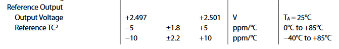
Fig 1. AD5752R DAC, Voltage Reference Specification
Frequency/Timing
We need a stable and precise frequency reference to enable accurate time-related signal generation and measurement. The FPGA daughter board has a 24MHz Clock module SIT9201AC-S3-XXE-24.000000G.
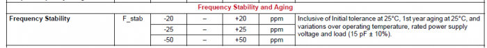
Fig 2. SIT9201AC-S3-XXE-24.000000G Clock Specification -50/+50 Part
At +-50ppm this is not a particularly impressive part, but it is fine for initial evaluation. If a higher precision/stability part is required, it can be added onto the spare bank of power and I/O pins on the FPGA daughter board.
Resistance
100 ohm and 5k precision resistors are provided as reference loads for closed-loop applications. These allow closed-loop gains to be measured and can be used in the Abitrary Circuit Emulation application to verify the emulation performance.
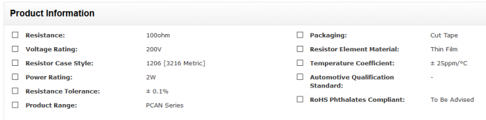
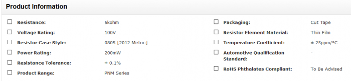
Fig 3. Precision Load Resistor Specifications
3. Capability to measure and to generate signals
ADC - LTC2387-16
A measurement chain consisting of a compensated potential divider, a buffer amplifier and an ADC driver feeds a LinearTech/ADI SAR 16bit ADC in each channel to provide a measurement capability. The potential divider can be connected to 0V dc, the 2.5V dc reference or the channel I/O port.
The limit of device operation is 15Msps.
DAC - LTC1668
The main signal generation capability is provided by a LinearTech/ADI 16bit DAC which provides a differential current to a dual op-amp and then on to the main port amplifier.
The limit of device operation is 50Msps.
4. Parameters for check and calibrate
ADC operation for calibration - general notes
The following parameters and methods were used to gather ADC signal records for calibration use.
- ADC conversion - initiated by the FPGA driving the ADC LVDS CVN Clock at 2Msps
- ADC 16bit data - ADC LVDS receive data is clocked into a double data rate (DDR) decoder and stored into a record buffer.
- ADC record - is 1024 samples * 0.5us = 512us duration
- ADC Test Pattern - a control is provided to force the ADC to provide a known test pattern
The Schematic for the FPGA ADC management arrangement is shown below

Fig 4. Schematic of the present FPGA ADC system, including DDR decoder, Offset removal, sample store and timing manager state machine.
ADC - Known Test Pattern
The LTC2397-16 has a test mode pattern which in the 2 Lane LVDS receive mode format is 0xCC3F Hex or -13249 signed decimal.
Here is the result of a 1024 ADC sample read record.
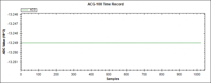
Fig 5. 1024 Samples with the ADC set to test pattern mode.
ADC Chain - Input Offset
The ADC measurement signal chain is connected to 0V via a suitable termination.
In this case the average ADC chain offset is around 189 counts out of a full scale range of -32768 to +32767

Fig 6. 1024 Samples with the ADC chain connected to 0V via a suitable termination
ADC Chain - Gain
The ADC measurement signal chain is connected to 0V and 2.5V low impedance reference voltages and the V/bit calibration factor is then calculated. This next screen shot shows a confirming measurement of the 2.5V reference voltage after the 2 ADC calibration factors have been applied.

Fig 7. 1024 Samples with the ADC chain connected to the 2.5V dc reference
ADC Chain - Noise floor test
The ADC measurement signal chain is connected to the 0V reference and a 32768 point sample record is collected. After removal of any dc the record is processed by an FFT with a Blackman-Harris window and scaled such that a sine-wave of full-Scale amplitude would be 0dB.

Fig 8. 0V Reference noise floor measurement using a windowed 32768 point FFT with 0dB representing the ADC full-scale amplitude
and the associated time-domain noise floor signal showing a maximum noise envelope of -8 to +3 counts.

Fig 9. 0V Reference time domain noise measurement
DAC Chain operation for calibration - general notes
The following parameters and methods were used to generate DAC signals for calibration use.
- DAC arrangement - There is 1 main DAC per channel and 1 secondary DAC for use in some applications. The main DAC provides a differential current to a dual op-amp and then on to the main port amplifier.
- DAC Data - because of a limitation on I/O pins on the FPGA daughter card, a 16bit data bus is used and 3 of the 4 DACs have latches to allow the each DAC to hold its data from the DAC data bus. The 4th DAC is connected directly to the DAC data bus. When all 4 DACs have the correct data presented, a conversion signal can be applied.
- DAC conversion - initiated by the FPGA driving each of the 4 DAC clock signals simultaneously or independently at a rate of 8Msps.
- DAC data - is a combination of a DC/Offset value, a signal generator value and a value computed by the feedback controller DSP block.
DAC Chain - Offset calibration
By setting various modes, setting a couple of trial DAC values and using the calibrated ADC to measure the resulting port voltage levels, we can determine the DAC dc trim values to ensure the port output is sensibly zero in it's quiescent state, as shown in the measurement below. The Y scale is +-3mV, measured value is < 1mV.

DAC Chain - Gain calibration
By setting various modes, setting a couple of trial DAC values and using the calibrated ADC to measure the resulting port voltage levels, we can determine the DAC V/bit gain values to allow the setting of precise dc voltage levels. The following screen shot shows the measurement summary for setting a value of +1Vdc after DAC chain offset and gain calibration factors have been applied.
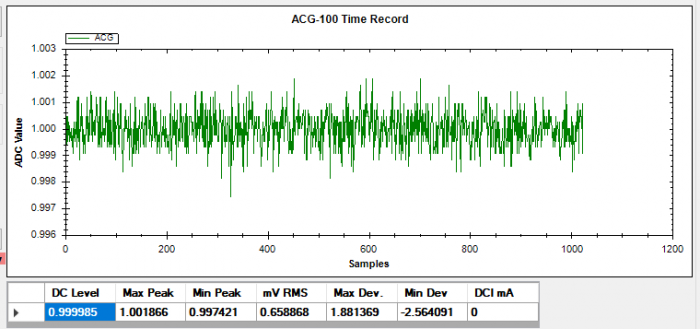
Fig 11. Measurement after DAC chain calibration of the port voltage for a +1Vdc setting.
Various Mode balances and trims
Further calibration measurements are taken to calibrate additional circuitry that might be used for more complex architectures.
5. External Confirming measurements
The following table shows a set of results for various set voltages. For each set voltage the calibrated ADC measurement and a reading from an independent DVM connected to the User Port are taken.
| Set Voltage | ADC Chain Self-Measurement | Error(mV) | External DVM Measurement | Error(mV) | ||
| -4 | -4.0018 | -1.8 | -4.002 | -2 | ||
| -2 | -2.0011 | -1.1 | -2.001 | -1 | ||
| -1 | -1.0009 | -0.9 | -1.001 | -1 | ||
| -100m | -100.1m | -0.1 | -100.4m | -0.4 | ||
| 0 | -0.0002 | -0.2 | -0.0005 | -0.5 | ||
| +100m | 99.8m | -0.2 | 99.5m | -0.5 | ||
| 1 | 0.9999 | -0.1 | 0.9997 | -0.3 | ||
| 2 | 2.0004 | +0.4 | 2.001 | +1 | ||
| 4 | 3.9992 | -0.8 | 4.000 | 0 |
Table 2. Set Voltage, ADC Chain self-measure, External DVM measure and mV errors
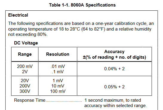
Fig 12. Fluke 8060A DC Voltage specifications.
6. Discussion
DAC chain DC Voltage setting and ADC chain measurement accuracy
The self-measurement is always within +-1mV of the DVM reading, and of course the self-measurements only take only 512 us compared to 1second taken by the DVM.
In simplistic terms it looks reasonable to claim a setting and measuring capability of +-0.1%+-1mV for the testing so far and there is always the possibility to refine the calibration processes further. To take into account the DAC reference error and apply further averaging.
ADC Chain Noise floor
At around -120 dB when measuring the 0V reference, the noise floor is a bit higher than the LinearTech/ADI published ADC specification of around -128 dB. But, the present design does not yet have any significant filtering and the measurement chain consists of a medium impedance resistor divider followed by a wide-band buffer op-amp and an ADC driver in an open electrical environment. This probably compares to an optimized laboratory measurement for the vendor data. Pending optimization of the measurement chain filtering and possible decimation filtering, the -120 dB Noise floor with no discernible spurious components is more than acceptable.
Thank you for your interest.
Next up - Will be Signal Generators.- Comments
- Write a Comment Select to add a comment

The ADC measurement signal chain is connected to 0V via a suitable termination.Don't assume that ADC voltage offsets are always positive; they can be negative, in which case a 0V input will be saturated as an ADC count of zero.

Hi jms_nh,
Thank you for my 1st comment. All the calibration calculations are based on signed maths and the ADC chain is designed to accommodate a -7.5V to +7.5V i/p range and to produce an ADC output code in the range of -32768 to +32767. The ADC Chain offset correction is also applied as a signed value.
No assumptions are made on either the sign of the offset or the sign of the gain constant. One thing I am guilty of is referring to ADC and DAC offsets and gains when in fact I really mean the ADC chain and the DAC chain rather than the ADC and the DAC in isolation. I will update the blog to clarify that.
In fact, 1 of the 2 unit channels has a +ve offset and the other a -ve offset and all is processed ok.

Some images are missing, not sure what happened but it looks like they would need to be uploaded again...
OK Stephane, thanks for letting me know. I noticed yesterday that some images on Blog 7 were OK in edit mode, but not in preview mode and had to be re-done.
Not sure why this is happening. If you notice a pattern, please feel free to let me know so I can try to address the issue. Thanks!
Looks like Blog 5 suffered from the same issue, I'll reload the images.
To post reply to a comment, click on the 'reply' button attached to each comment. To post a new comment (not a reply to a comment) check out the 'Write a Comment' tab at the top of the comments.
Please login (on the right) if you already have an account on this platform.
Otherwise, please use this form to register (free) an join one of the largest online community for Electrical/Embedded/DSP/FPGA/ML engineers:


