


Attached is an RF-DAC output of a modulated IQ signal.
Signal is generated with an FPGA with a simple "F/4" I-Q modulator. The RF-DAC sample frequency is 4700 MHz. The modulated carrier is therefore 4700 MHz/4 = 1175 MHz. My signal of interest is a Nyquist image at 2Fs - Fs/4. Ie: (2*4700) - (4700/4) = 8225 MHz.That's fine, the signals are where I expect them. However. I'm not sure what the artefact lobes are around the Fs, 2Fs, 3Fs indicated with a red line and question mark are.
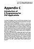
I have drawn a red line to show the NRZ sinx/x response (DAC is in an RF mode).
Thanks
DavidDAC Response.JPG

It looks to me like the signal was generated at baseband at half the sample rate, then mixed up to fs/4 without sufficiently suppressing the nearest image. The artifact you're seeing is the signal image pierced by the null of a sinx/x response. They're spaced 2x closer than the current sample rate probably because they were generated or mixed at the lower sample rate.
There are probably other ways to get there, but that's one way. In any case, I think the two-lobed "artifact" you're seeing is another signal image with a null through it.
BTDT. Some better filtering at an earlier stage can help get rid of those if they're problematic, otherwise if your IF filtering is really good they may be a non-issue.
DAC Baseband Response No Modulation.JPGDAC Baseband Response.JPG
The signal was created as a carrier of Fs/4, ie: +1, 0, -1, +1.....
There is no mixing, this is all digital, right out of the DAC. Attached is a zoom in of the baseband carrier (Fs/4) with and without modulation.
The multiplication by +1, 0, -1... is the mixer, so, yes, you are mixing from baseband to fs/4 that way. It is a very common way to do the mix, and then take an image at a higher frequency to avoid an rf mixing step. Regardless of how it was done, it appears that somewhere along the way the signal was at a lower sample rate and half of the images got split by nulls to form the "artifacts" that you're seeing now.
Apologies, you are correct. That is how I am mixing it up. and yes, the idea is to take an nth image which looks like it could work, just not sure about that artefacts messing up my spectrum/emissions.
Sorry, could you explain what, "half of the images got split by nulls" means please?
Attached is a diagram of what I am providing to the DAC.
In the FPGA I have a block of code that produces I and Q outputs in parallel. They are root-raised cosine filtered and this produces 4 samples per symbol (4x interpolating perhaps this is called). So my block produces 4 I and 4Q samples for every symbol.
Hopefully the diagram will explain what I'm doing.
Many thanks

Based on your diagram it looks like you are mixing one sample of signal with 4 samples of sin/cos. am I right
Correct.
I "multiply" (xor) I with "1100"
I "multiply" (xor) Q with "1001"
then I add them together. That makes: 2, 1, 0, 1. And if you take the DC offset away, that is 1, 0, -1, 0.
That looks wrong to me. Mixer inputs should be at same sampling rate.
The mixer must use one sample of each to produce one output.
your mixing as such will cause lobes. You still may demodulate but I see it wrong mixing
When you say lobes, is that harmonics because of the crude sin wave? Or is a lobe something different? I'm not sure how you can avoid this issue when you create an IF of +1, 0, -1, 0 ? Thanks.
I don't understand your message that "the mixer must use one same of each to produce one product."
I beleive that the mixer is running at the sampling rate, First sample will be 1, then 0 then -1, then 0. So that gives me the IF to be Fs/4.
Not sure if I have not presented my implementation correctly or you get that, but you're saying its wrong? My 1100, 1001 numbers are sequential. Hard to convey in words perhaps.
Your mixer is not crude first. It is well known. You need to mix your signal with frequency sample by sample. one sample of signal multiplies by one sample of frequency. hence for every cycle of sin/cos you should have four samples of signal going into mixer.
It is ok to have that pattern of frequency generation but you are applying it wrong.
Hmmm, I think you are saying I need to implement B in the attachment? If so then that presents a problem because I have root raised cosine filtering and each data symbol has 4 (interpolated) sub-samples/symbol.
I'm pretty sure that I tried option A in the past and it was not demodulated...
I guess you are not that clear. Do you mix before or after up4.
either way the stream (be it named samples or symbols) that goes to mixer must mix one sample at a time with one sample cos/sin
I hope I'm not frustrating you.. I don't know what you mean by up4. I have updated the diagram to show when these "samples" go to the DAC.
Is there some text on the web I could study please?
up4 is interpolate by4 (RRCos filter module in your case).
you can apply mixing either before or after interp4 but affects target frequency value. you will get Fs/4 depending on Fs value at the point of mixing
It could be false alarm if you are mixing after upsampling by4. So ignore my comments otherwise. option A is correct...
Thanks for the help. I only found out about this scheme by a few sentences in a paper on the web. Is there some online text that discusses this method please? Is there a formal name for this scheme that I could Google? Thanks for the help again.
You and someone else on this forum have said that this technique is well known but I have not found anything on the web. I may be that I don't know what to search for. Is there some text on the web I could read up on this please? Thanks.
it is just mixer (e.g. for quadrature demod) and specifically it generates frequency without LUT as f = Fs/4
Not sure if it helps. But this is how I would implement option A.
The DAC multiplexes the 4 inputs 1 at a time.
If I(0) to I(3) are the successive parallel four samples per symbol then you need to multiply by : 1,0,-1,0 (not sure why you use 1,0,0,1)
and Q(0) to Q(3) by : 0,1,0,-1
so the first sample I(0) always multiplies by 1, I(1) by 0 ...etc.
as such your design looks ok to me and practical implementation.
You may have to check your interp by 4 is cutting off images(lobes) well enough.
I've been away all day and just coming back to this. Kaz is on the right track in that I think you're not implementing the mixer correctly and you're winding up with images reflected from both positive and negative frequencies. This also explains why you have a LOT of energy sticking up at your mixing frequency, which shouldn't be there at all.
If you do a web search on "fs/4 mixer" there should be several good references. When I do this search the notes at dspguru and e2e.ti.com are pretty good. There are some interesting subtleties that can be applied with this trick, but generally you are mixing your complex baseband signal with a complex mixer that has a period of four samples/cycle. Each baseband signal sample gets multiplied by a mixer output. The mixer outputs are, usually, for a clockwise rotation to mix "up":
I:+1,0,-1,0,+1,0,-1,0,+1...
Q:0,-1,0,+1,0,-1,0,+1,0...
If you plot that as a polar vector that's rotating, the sample points are on the axes. If you rotate the sample points 45 degrees, which is a perfectly fine thing to do, you get:
I:+1,+1,-1,-1,+1,+1,-1,-1,+1...
Q:+1,-1,-1,+1,+1,-1,-1,+1,+1...
The advantage of the first method is that you can skip a lot of multiplies and adds by throwing out the terms multiplied by zero. When this is done in hardware it is usually done this way to save gates. The gain of the mixer in this method is 1. In the second method there is a little bit of numerical gain, specifically sqrt(2), which can be useful in some cases for numerical precision management.
Either way works just fine, but it doesn't look to me like either one of those is what you're doing.
Thank you for the reply. Yes, I'm using +1 and -1 for the multiplier as this results in a simple XOR. I have changed the FPGA to option A as I discussed with KAZ in this thread. I clocked the DAC at 500 MHz. This is the result. Is this what you would expect? I think it is FS4_DAC500M.JPG
The DAC is now in NRZ mode so the top of the signal droops a bit.
My concern with this scheme is that its harder to band pass filter the Nyquist image of interest. I also don't think I will be able to get this to work at 8.2 GHz because the symbol rate will be too high (I only need about 200 MSym/s). I'd have to take a high Nyquist zone band and there will be little amplitude there. With my "Fs/16" I could get to 8.2 GHz with NZ4.
Alternatively I could low pass filter the base-band image and use an LO to mix up. But because the IF is so low (125 MHz) the unwanted mixer image will be too close to filter out. Ie, 8325MHz LO gives images at 8200 and 8450 MHz.
Any comments welcome how you practically use the Fs/4, how I could get this to work at ~8.2 GHz... Thanks
Yes, the spectrum in that pic is what I would expect to see. That looks a lot better.
If you have the processing bandwidth to upsample the baseband signal by a factor of 2 or 4 before mixing up to fs/4, the images will be separated by 2x or 4x more than they are in the latest pic. Upsampling as much as you can stand before mixing up digitally is usually worthwhile if you can afford the processing.
Sorry, could you explain how I upsample please? Is that "zero-stuffing" where I take the modulated signal, lets call that sample sequence S0, S1, S2, S3... and "over-clock" it to make it S0, 0, 0, 0, S1, 0, 0, 0, S2, 0, 0, 0...? That I think is followed by a low pass filter.
But I should point out that the symbol data has already been RRC filtered and produces 4 outputs per symbol (see a previous attachment). I therefore believe it already has a 4x interpolating filter applied.
I'm pretty good with FPGAs, but a DSP beginner!
I was wondering about just sampling my output at 4x the rate with the DAC, feed the same sample to the DAC every 4 DAC clock cycles (not sure if that works)
This is where Simulink would be handy I guess.
Rick's book should have some good treatments on upsampling, also called interpolating or interpolation. There are many techniques, but for a modulator it will likely need a good interpolating filter as well. Zero-stuffing followed by a filter or sample repetition followed by a filter can both be made to work, but doing either without filtering will yield some undesirable effects for a modulator.
Thanks.
OK, so attached are 2 sets of waveforms. The top set is my amended implementation that got rid of those artefacts and I think is what is meant by Fs/4, but as discussed, that is too fast a symbol rate and the unwanted images will be hard to filter.
The bottom diagram I think is what you're saying I need to do. That is interpolate (in this case by 16).
I think I need to discard the core's x4 RRC output and create my own x16 RRC output. I'm assuming I can make the up-sampler's low pass filter a RRC filter...
My symbol rate is ~ 100 MSym/s so I guess I will be needing a polyphase FIR. I'm using a Xilinx Virtex-7 FPGA and have looked at the FIR Compiler. I don't see how you get the choice of Polyphase filter, or how you can get x16 output from it.
Presumably I can use Simulink System Generator to trial this? Fs-16.JPG
Can Simulink implement polyphase interpolators I could use off the shelf? (never used Simulink/System Generator so more learning there).
Hi,
100Msymb/s x 16 = 1600 Msps. Can you run that fast.
In your first design with up4 you used 4 parallel streams into DAC. Can you do 16 parallel streams into DAC.
Yes. In actual fact I think I need x32 to run the DAC at 4700 Msps and I have demonstrated the hardware interface runs at this speed. You use the FPGA's OSERDES blocks.
The DAC gives the FPGA a clock of fDAC/8 (= 587.5 MHz). You then use 4 lanes of OSERDES in 8:1 mode (DDR) and so now you clock your 32 samples in parallel at a leisurely 146.875 MHz.
The bit I'll be stuck on is creating a polyphase filter x32...
Symbol rate = fDAC/32 = 146.875 Msym/s. 146.875 Msym/s * 32 = 4700 MSa/s to the DAC.
The reason for running the DAC so fast is to use Fs/4 and Nyquist zone 4 (4700*1.75) to get my signal where I want it at 8.225 GHz.
You can design RRC upsampling by 32 manually or through ip cores.
For core you don't need to tell it for polyphase as it knows how to implement it- hopefully
Hello David,
The span is 10GHz with 8.25GHz center frequency, therefore each horizontal division is about 825MHz.
The unwanted lobes are roughly +/- ~200MHz around the sampling frequency.
That means they are image of a ~200MHz signal.
What is odd that you can see the sampling clock which should have been nulled, since it isn’t, then there is leakage or bleeding of the sampling clock.
Best regards,
Shahram Shafie
The DAC has several modes: NRZ, RTZ, RF etc. The DAC is in RF mode. The datasheet states that a weakness of RF mode is Fs clock spurs. Indeed, they disappear when I switch to NRZ. Here is the baseband response in NRZ and the lobes are increased.
DAC Baseband Response NRZ.JPGDAC Baseband Response NRZ No Modulation.JPG
My IF carrier is made simply from +1, 0, -1, 0.... So its crude. But that would mean I guess, components at 3rd, 5th etc. That would be 3525 MHz. But in another reply above I turned off the modulation to show just the carrier. Thanks.
Its an e2V RF DAC (they don't have many in the range - same device just different max sample rates) but to be honest, I see the same issue with a completely different DAC that has not got RF mode. I see the same issue in NRZ mode. Its a problem of my doing.


