


ADC Clock Jitter Model, Part 1 – Deterministic Jitter
Analog to digital converters (ADC’s) have several imperfections that affect communications signals, including thermal noise, differential nonlinearity, and sample clock jitter [1, 2]. As shown in Figure 1, the ADC has a sample/hold function that is clocked by a sample clock. Jitter on the sample clock causes the sampling instants to vary from the ideal sample time. This transfers the jitter from the sample clock to the input signal.
In this article, I present a Matlab ADC jitter model. The model’s inputs are an arbitrary ADC input signal vector and a time-jitter vector. The input signal can be a sine, multiple sines or anything you want to try. The time jitter can be sine, Gaussian, filtered-Gaussian, etc. The model is useful in giving a sense of how input signals and their spectra are affected by jitter, which we’ll see in some examples.
Random jitter, or phase noise, is inherent in any oscillator. In the frequency domain, it appears as a spreading of the carrier energy that is referred to as sidebands, but these sidebands are not discrete. Deterministic jitter is caused by real-world implementations where, for example, unwanted clock signals may be coupled to power or ground traces of the sample clock oscillator, causing discrete phase sidebands. Since the discrete jitter case is simplest, we’ll begin with it here in Part 1. Then we’ll cover random jitter in Part 2.
This article is available in PDF format for easy printing.
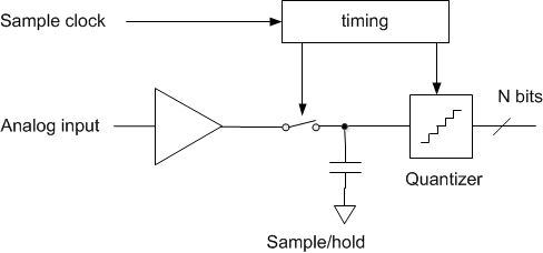
Figure 1. Sample clock and ADC sample/hold function
Example 1.
The Matlab function adc_jitter is listed in the appendix. Before describing how the function works, we’ll use it to perform a simulation using a sine input and sinusoidal jitter on the sample clock.
We have to create the analog input signal and the time jitter vector before we call adc_jitter. First, we define the ADC sample rate, input signal frequency, jitter frequency, and jitter amplitude. Also, we define the simulation sample rate, which is twice the ADC sample rate.
    fs_adc= 100E6;             % Hz ADC sample rate
    f0 = 10E6;                 % Hz ADC input sinewave frequency
    fm = 1.9E6;                % Hz jitter freq
    A = 200e-12;               % s peak jitter of sample clock
    fs= 2*fs_adc;              % Hz simulation sample rate
Next, define the analog input sinewave x and the jitter sinewave dt. The units of the jitter amplitude is seconds. We compute the jitter in samples = dt/Ts, then call the Matlab function adc_jitter. Finally, we quantize the output to 10 bits.
    Ts= 1/fs;                        % s sample time
    N= 4096;
    n= 0:N-1;                        %  sample index
    x= sin(2*pi*f0*n*Ts);            %  adc analog input
    dt= A*cos(2*pi*fm*n*Ts);         % s sinusoidal jitter of sample clock
    dsample= dt/Ts;                  %  jitter in samples
    y= adc_jitter(x,dsample);        %  add jitter to x
    nbits= 10;
    y= floor(2^(nbits-1)*y)/2^(nbits-1);    % quantize to nbits
The output y is at the fs_adc sample rate of 100 MHz. An eye diagram superimposing all cycles of the ADC output sinewave is plotted in Figure 2. The jitter is just visible. A zoomed version is shown in Figure 3. The jitter is equal to that of the sample clock, i.e. 200 ps peak or 400 ps peak-to-peak.
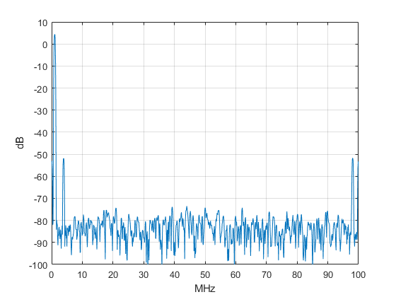
The spectra of the ADC input and output are shown in Figure 4. The input spectrum is a pure tone. The output spectrum has sidebands due to sample clock jitter at fm= 1.9 MHz. You can also see the quantization noise floor at the bottom edge of the plot.
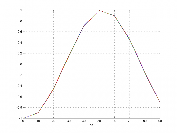
Figure 2. Eye Diagram with time axis showing one cycle of ADC output signal.
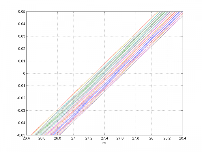
Figure 3. Zoom of Eye Diagram at 200 ps per division.
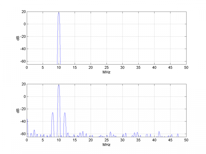
Figure 4.Top: Spectrum of ADC input signal.
Bottom: Spectrum of ADC output signal psd(y,N/4,fs_adc/1e6,flattopwin(N/4))
How the Model Works
The Matlab function adc_jitter(x,dsample) is shown in the appendix. The function’s inputs are the ADC analog input x(n) and the sample clock jitter in samples, dsample(n).
In Example 1, we assumed a time jitter waveform dt(n) that was a sinusoid with frequency fm and amplitude A seconds. For every sample n, we had dt(n) = A*cos(2πfm*nTs). We then computed jitter in samples as dsample(n) = dt(n)/Ts.
Thus, for every ADC sample x(n), the sampling instant was offset by dt(n). As shown in Figure 5 for a single sample, this time offset means that the sampled analog voltage is offset from the ideal value. The model needs to estimate this voltage, shown as the red asterisk. It does so by interpolating between samples of the input voltage. We need to use a variable interpolator because each value of dt(n) is unique; i.e., the interpolation index dt(n)/Ts is not a constant.
Since we are normally interested in small values of dt, we could use a linear interpolator. However, we can get more accurate results over a wider range of jitter amplitude by using a polynomial (e.g. parabolic or cubic) interpolator [3, 4]. The function adc_jitter uses parabolic interpolation.
Referring again to Figure 5, note that if the input signal is sinusoidal, the jitter dt moves the sample point in phase by 2π* dt/Ts. Thus the jitter on the sample clock amounts to phase modulation of the input sinusoid. To the extent that our model’s interpolation is accurate, it performs pure phase modulation.
A few details: First, the inputs x and dsample of adc_jitter are sampled at twice the ADC sample rate of fs_adc. Once the interpolated values are calculated, they are downsampled by two, to fs_adc. The reason for this is to account for the bandwidth of the interpolator (see appendix). Input signal frequency components above fs_adc/2 will be aliased. Second, rather than using interpolation index of dt/Ts, we use dt/Ts + 0.5. This prevents having a negative interpolation index when dt is negative. Finally, note that in all of this we did not generate a sample clock; the model doesn’t need a sample clock, just the vector dsample of jitter in samples.
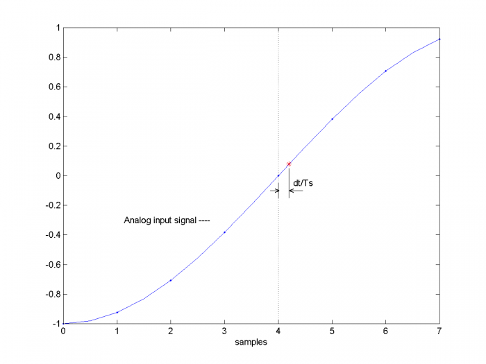
Figure 5. Effect of jitter on sampling
Calculating Sidebands Caused by Jitter
One way to check the model is to calculate the jitter sidebands and see if the model matches the calculation. We begin by noting that the jitter sidebands represent phase modulation. We then have [5]:
$$\phi^2=\frac{2\cdot SSB\, power}{carrier\, power}\qquad rad^2$$
where ϕ is rms phase relative to carrier phase in radians and SSB power is the power of one sideband. We can rewrite the above as:
$$\phi^2=2\cdot 10^{PSSB/10} \; ,$$
where PSSB is the power of one sideband in dB relative to the carrier power (dBc). We have assumed the level of higher-order phase sidebands is negligible. Taking the square-root,
$$\phi= \sqrt{2} \cdot 10^{PSSB/20}\qquad rad\;rms$$
Thus,
$$PSSB = 20log_{10}(\phi)-3.01\qquad dBc \qquad (1)$$
Phase jitter in radians and clock jitter in seconds are
simply related by:
$$\phi=2\pi \frac{\Delta t_{rms}}{T_0}=2\pi\Delta t_{rms}f_0 \qquad (2) $$
where Δtrms is the rms clock jitter in seconds, T0 is carrier period, and f0 is carrier frequency. For an ADC, the jitter Δtrms in Equation 2 is a constant vs. f0. Thus for increasing f0, Δtrms becomes a larger and larger fraction of T0, causing ϕ to grow linearly vs. f0. Substituting for ϕ in equation 1, we have:
$$PSSB = 20log_{10}(2\pi\Delta t_{rms}f_0) -3.01\qquad dBc \qquad (3)$$
Example 1 used $\Delta t_{rms}= 200/\sqrt{2} $ ps and f0 = 10 MHz, so we expect PSSB = -44.04 dB. Checking Figure 4, we see good agreement.
We can also relate the ADC output’s sideband level directly to the sideband level of the sample clock. For the sample clock, we can modify Equation 3 as follows, where we use the fact that the jitter on the carrier and the sample clock are both Δtrms:
$$PSSB_{clk} = 20log_{10}(2\pi\Delta t_{rms}f_s) -3.01\qquad dBc $$
Combining this with Equation 2, we then have:
$$PSSB_{signal}= PSSB_{clk} -20log_{10} (f_s/f_0) \qquad (4)$$
In other words, the signal sidebands are lower than the sample clock sidebands by $20log_{10}(f_s/f_0) $ dB.
Example 2.
Equation 3 shows that the sideband level due to jitter varies as 20*log10 of the analog input signal’s carrier frequency. We can illustrate this by letting the input equal the sum of two sinewaves at 10 MHz and 40 MHz. Then the sideband level should be 20*log10(4) = 12 dB higher at 40 MHz than at 10 MHz. We use the same code as above, with ADC input x replaced by:
x= sin(2*pi*f0*n*Ts) + sin(2*pi*4*f0*n*Ts); % adc analog input
The resulting input and output spectra are shown in Figure 6. As expected, the sidebands at 40 MHz are about 12 dB higher than those at 10 MHz. The second-order phase sidebands are also visible. Note that the input signal amplitude is about +/-2 Vpp, so quantization level is effectively 11 bits.
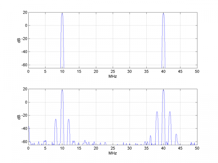
Figure 6.Top: Spectrum of ADC input signal. Bottom: Spectrum of ADC output signal
Example 3.
In this example, we’ll phase-demodulate the ADC output, and compare the demodulated phase jitter to the expected jitter. We set the input frequency and jitter as follows:
    f0 = 35E6;        % Hz ADC input sinewave frequency
    A= 0.6e-9         % s  peak jitter of sample clock
This gives the spectrum of Figure 7. Now let’s calculate the expected phase jitter of the output.Modifying Equation 2 for peak-to-peak phase jitter, we have:
$$\phi_{pp}=2\pi\Delta t_{pp}f_0 $$
So we expect ϕpp = 2π*1.2E-9*35E6 = .2639 radians pp or 15.12 degrees pp. If we phase-demodulate the ADC output and plot Q vs. I, we get the result shown in Figure 8. As expected, the peak-to-peak phase jitter is about 15 degrees. It is worth noting that even for the relatively large phase excursion of this example, the model produces almost pure phase modulation on the ADC output.
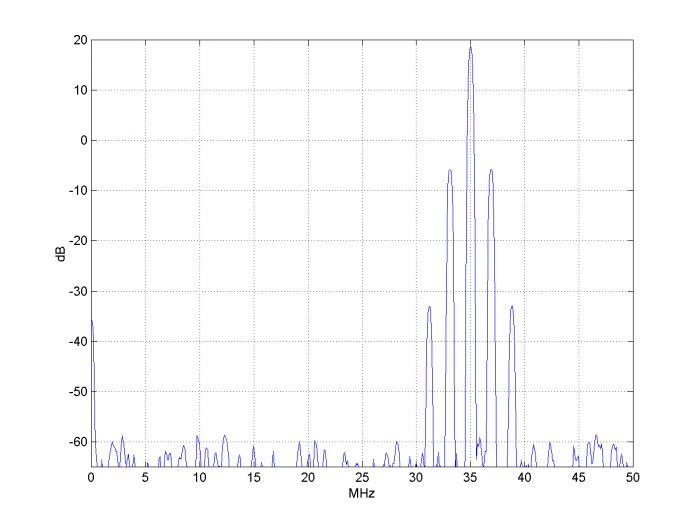
Figure 7. Spectrum of ADC output for f0 = 35 MHz and sample clock peak jitter = 0.6E-9 s.
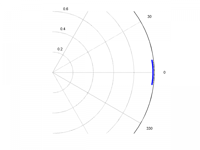
Figure 8. Q vs. I of phase-demodulated ADC output signal for f0 = 35 MHz
and sample clock peak jitter = 0.6E-9 s.
Example 4.
We can also model a non-sinusoidal input to the ADC. Figure 9 shows the spectrum of a modulated pulse with approximately rectangular spectrum applied to the ADC, where we have set:
    f0 = 30E6;        % Hz ADC input center frequency
    fm= 3.9E6;        % Hz jitter freq
    A= 100e-12        % s peak jitter of sample clock
The ADC output has jitter sidebands offset from the signal by +/- fm = +/- 3.9 MHz.
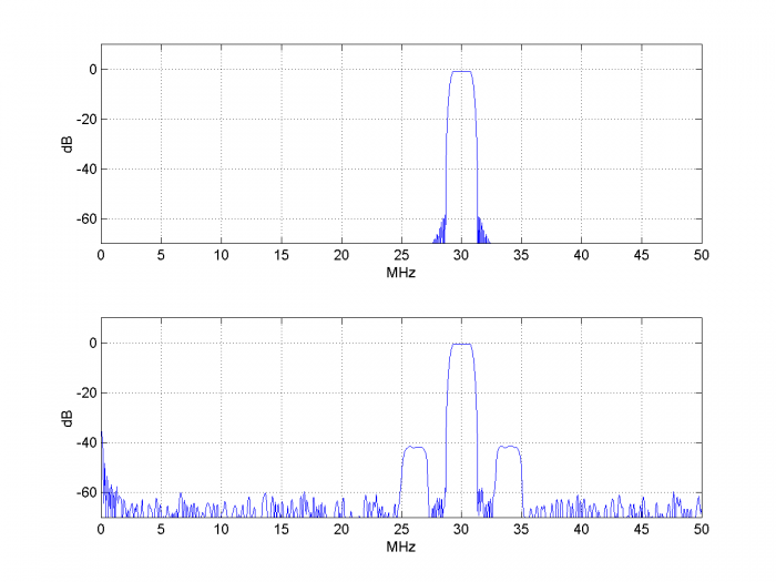
Figure 9. Top: Spectrum of ADC input signal. Bottom: Spectrum of ADC output signal.
References
1. Kester, Walt, Ed., The Data Conversion Handbook, 2005, Newnes, Ch 2.
http://www.analog.com/en/education/education-library/data-conversion-handbook.html
2. Brannon, Brad, “Sampled Systems and the Effects of Clock Phase Noise and Jitter”, Analog Devices Application Note AN-756, 2004
http://www.analog.com/media/en/technical-documentation/application-notes/AN-756.pdf
3. Erup, Lars; Gardner, Floyd M. and Harris, Robert A., “Interpolation in Digital Modems – Part II:Implementation and Performance”, IEEE Transactions on Communications, Vol 41, No. 6, June 1993.
4. Rice, Michael, Digital Communications, a Discrete-Time Approach, Pearson Prentice Hall, 2009, section 8.4.2.
5. Goldberg, Bar-Giora, “Phase Noise Theory and Measurements:A Short Review”, Microwave Journal, Jan 1 2000. https://www.google.com/search?q=%2C+Phase+Noise+Theory+and+Measurements%3A+A+Short+Review&oq=%2C+Phase+Noise+Theory+and+Measurements%3A+A+Short+Review&aqs=chrome..69i57.4669j0j8&sourceid=chrome&ie=UTF-8
Neil Robertson April, 2018
Revised March 2019
Appendix Matlab Function adc_jitter
Figure A.1 shows the interpolation of the input signal about mu = 0.5 + dt/Ts = 0.5 + dsample, where dsample is signed. Figure A.2 shows the frequency response of the interpolator for mu = 0.5. Because the output is downsampled by two, only the frequency range from 0 to fs/4 is used.
%function y= adc_jitter(x,dsample)  4/15/18  Neil Robertson
% Model ADC with jitter on sample clock, computing jittered samples by
% parabolic interpolation.
% Add jitter to input signal x, then downsample by 2.
%
% x          input signal vector
% dsample    input jitter vector, jitter in samples
% y          output signal vector with jitter, sample freq = 1/2 of input fs
%
function y= adc_jitter(x,dsample)
if length(x)~=length(dsample)
    error('x and dsample must be of equal length')
end
N= length(x);
V= x;
% find jittered samples using parabolic interpolation
mu= 0.5 + dsample;                % mu = 0.5 +/- jitter
a= 0.4;                           % interpolator free parameter
b1= [-a a+1 a-1 -a];              % Farrow coefficients
b2= [1 -1 -1 1];                  % Farrow coefficients
u= zeros(1,N);
for n= 4:N;
     Vreg= V(n:-1:n-3);        % reg holding 4 samples of V, current sample first
     u(n)= Vreg(3) + mu(n)*( sum(b1.*Vreg) + mu(n)*a*sum(b2.*Vreg));
end
y= u(1:2:end);                    % downsample by 2
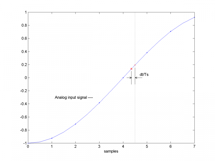
Figure A.1 Variable Interpolation. mu= 0.5 + dt/Ts = 0.5 + dsample.
(example with dt/Ts negative)
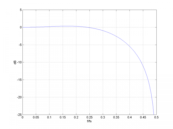
Figure A.2 Parabolic Interpolator Frequency response for mu = 0.5 and a = 0.4.
- Comments
- Write a Comment Select to add a comment
Hi Sir, what do we exactly mean by jitter per sample and what are farrow coefficents?

Hi Somu29,
I compute the jitter in samples as:
dsample= dt/Ts;
So I should have called it "jitter in samples".
Units are s/(s/sample) = samples. I updated the post to fix this error.
A Farrow interpolator is an efficient structure to implement a parabolic or cubic interpolator. The coefficients are defined in references 3 and 4.
regards,
Neil
Hi Neil,
There is a slight timing snag in jitter function.
This can be seen by plotting jitter noise versus timing jitter:
plot(dt(1:2:end),x(1:2:end)-y,'.')
The jitter noise near dt=0 should be close to zero, but it's not.
This issue may be relevant a time-interleaved ADC behavioral model.
Best regards,
Marko
Marko,
OK, I have a better answer. The issue you found is due to a delay between the input x and the output y of the function adc_jitter. A way to get around this problem is to call adc_jitter twice: The first time, you use the desired jitter; the 2nd time you use a jitter vector that is all zeros. Then the error due to jitter is the difference of the two outputs, called y and y0: error = y - y0.
Below are plots of error and dsample vs sample number and error vs. dt. As desired, error is zero when dsample or dt is zero.
Here is the code. Note I changed f0 and fm from the values used in the post.
% alignment_test.m   1/24/20 nr
% call adc_jitter.m for sinusoidal jitter and jitter = 0
% This allows plotting error due to jitter
fs_adc= 100E6;      % Hz ADC sample rate
f0 = 5E6;           % Hz ADC input sinewave frequency
fm = .55E6;         % Hz jitter freq
A = 200e-12         % s peak jitter of sample clock
fs= 2*fs_adc;       % Hz simulation sample rate
Ts= 1/fs;           % s  sample time
N= 4096;
n= 0:N-1;           %   sample index
x= sin(2*pi*f0*n*Ts);         % adc analog input
dt= A*cos(2*pi*fm*n*Ts);      % s  sinusoidal jitter of sample clock
dsample= dt/Ts;               %   jitter in samples
y= adc_jitter(x,dsample);     %   add jitter to x
% case with jitter vector = all zeros
dsample2= zeros(1,N);
y0= adc_jitter(x,dsample2);
error= y -y0;
%
% plot error for 400 samples
plot(1:400,dsample(1:2:800),1:400,error(1:400)),grid
xlabel('sample'),ylabel('dsample (blue) and error (orange)')
figure
% plot error vs dt over all samples
plot(dt(1:2:end),error),grid
xlabel('dt (s)'),ylabel('error')
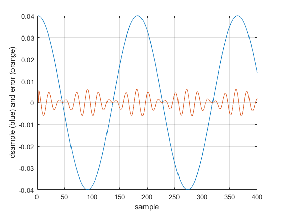
dsample (blue) and error due to jitter (orange) vs. sample number
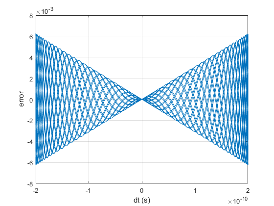
error due to jitter vs jitter dt over all samples
Neil,
Thank you so much for your quick response.
In your response code, the zero-jitter output y0 is x(1:2:end) delayed for 1.25 samples. In some modeling environments, an extra delay not desired.
Here are my thoughts solving the synchronization issue:
In adc_jitter.m, the data rate of dsample is doubled. If you delay dsample by one would mean 0.5 sample delay of jitter in the output y.
Changing two lines in adc_jitter.m would synchronize x(1:2:end) and y:
function y= adc_jitter(x,dsample)
...
mu= 1 + dsample; % mu = 1 +/- jitter
...
y= u(2:2:end); % downsample by 2
Any comments?
Best regards,
Marko
Marko,
Normally, the range of mu in a Farrow interpolator is 0 to 1. Playing around with mu, the interpolator does seem to function if mu = dsample or mu = 1 + dsample. For mu = dsample, mu can be negative, while for mu = 1 + dsample, mu can be > 1. In either case, the impulse response of the interpolator can exceed +/-1.
Also, for either case, the frequency response of the interpolator is no longer lowpass, but has a slight peaking for f > fs/4.
I have not looked at this closely, so there could be some unforseen problem with using mu= dsample or mu= 1+ dsample.
regards,
Neil
Neil,
Indeed, I've suspected that such filtering may distort data slightly.
I noticed that MATLAB DSP System Toolbox has a built-in fractional delay filtering function (dsp.VariableFractionalDelay) with LaGrange method of interpolation enabled.
In the function, the fractional delay can't be negative, but this can be circumvented.
Here's an example (with bandlimited random jitter):
fs= 100E6;          % Hz ADC sample rate
f0 = 2.5*pi*1e6;    % Hz ADC input sinewave frequency
A = 1e-11;          % Peak jitter of sample clock
Ts= 1/fs;                        % s sample time
N= 2048;
t= (Ts*(0:(N-1))).';
x= sin(2*pi*f0*t);
fc= 2.5e6; % Hz cutoff freq of noise filter
rng(25225255)
[b,a]= butter(7,2*fc/fs); % coeffs of noise filter
u= A*randn(N,1); % AWGN sequence
dt= filter(b,a,u); % filtered sequence = jitter of sample clock
dsample= dt/Ts;                  %  jitter in samples
fracDelay = dsp.VariableFractionalDelay('InterpolationMethod','Farrow','FilterLength',2);
qin = fracDelay(x,dsample+1); % fractional delay + 1 sample delay
reset(fracDelay)
qin = [qin(2:end);qin(1)]; % 1 sample advance
nbits= 12;
qout= floor(2^(nbits-1)*qin)/2^(nbits-1);    % quantize to nbits

plot(dt*fs,x-qin,'.')
xlabel('t_{jitt}*f_s')
ylabel('e_{jitt}')
set(gca,'Ylim',[-1,1]*A*fs)
Hi Neil
What about DAC jitter ? is it similar to ADC jitter?
I have built a model for the ADC jitter, do you think I can use it as DAC jitter?
Any idea?
thanks for your support
Amro_gonem,
I think you can use the same model for a signal source that uses a DAC. However, there is probably a more direct way to model source jitter. For example, if your source includes an NCO, you could add a phase signal to the NCO's accumulator. For sinusoidal jitter of frequency f0, the phase signal would be
dphi = A*cos(2*pi*f0*n*Ts).
regards,
Neil
Hi Neil
Thanks for your fast response, I appreciate it.
My work is all based on Matlab simulation, I am a bit confused if the ADC jitter model can be used as DAC jitter model? could you please explain why you think we can use it as DAC jitter model.
Assuming a NRZ DAC, the ideal output analogue signal of the DAC is a series of connected pulses with different amplitudes but with the SAME widths (Ts or sampling duration). Then if the DAC's clock is not ideal, then it causes either delay/advance in the next pulse. The resulted analogue signal is then a series of connected pulses with different amplitudes and with DIFFERENT widths. I am having a problem in simulating this DAC jitter in Matlab. Any ideas?
Thanks
AMRO
Amro,
You can view the DAC as two cascaded parts: a "jitter source" followed by a zero-order hold. You can't exactly model the zero-order hold. One way to model it would be to filter the signal with an FIR filter having a sin(pi*f*Ts)/(pi*f*Ts) response up to the highest frequency of interest.
The jitter source model cannot actually change the sample positions; it rather interpolates between the fixed sample instants using a jittered interpolation index.
You can model the jitter source the same way as for an ADC; the input is a series of samples and the ouput is a series of interpolated values that vary in amplitude due to the jitter.
On the other hand, it might be easier to introduce the jitter where the signal is generated. For example, if the signal generation involves an NCO, the jitter can be added there, as I already mentioned.
regards,
Neil
Thanks, I will give it a try.
What is the name of this filter? I believe it has a rectangular impulse response and sinc magnitude response.
regards
It's called a sinx/x response. Note if you have a sample rate of 400 Hz, if you use a boxcar filter b= [1 1 1 1]/4, it will have approximately the same response over 0 to 50 MHz as a DAC sampled at 100 Hz.
b= [1 1 1 1]/4;
[h,f]= freqz(b,1,256,400);
H=20*log10(abs(h));
plot(f,H),grid
axis([0 50 -20 5])
regards,
Neil
*50Hz
Thanks for your support, actually most of the time, we model the DAC as a quantization only, we ignore this filtering because of the discrete nature of matlab. In order to model this zero order hold operation, we must use two or more discrete values for one time domain sample. for example, if the input signal is:
x(n)=[0.1 0.2 0.3 0.4....]
the output of the DAC (ignoring quantization, and considering zero order hold):
x(t)=[0.1 0.1 0.1 0.1 0.2 0.2 0.2 0.2 0.3 0.3 0.3 0.3.....]
here I assumed that sampling duration Ts=4 matlab discrete samples.
funny solution ! because further matlab processing would be very complicated espically if OFDM is used
Regards
Hello,
Does your model simulate sampling clock power, i.e. slew rate?
If so, how?
thank you,
Dave
Dave,
The model assumes a perfect impulse train with added jitter as the sample clock. So no, it does not simulate sample clock slew rate.
regards,
Neil
Hi! I'm Andre. Congratulations about this tutorial and this site. I'm trying to use this and I have one doubt. I have a complex signal, with its real and imaginary parts. Do you know if I can use this same matlab code? Do I have to use it to real part of my signal and then to the imaginary part, and after that sum the real part with the imaginary one? Or I can perform the script to the complex signal (real and imaginary part since the beginning of the code)?
Thank you so much for your attention!
Andre,
I think you can use the adc_jitter.m function for a complex signal. Here is an example, where I'm assuming that the I and Q channels have exactly the same jitter amplitude and phase. The input is a complex sinewave at 1 MHz, fs_adc is 100 MHz, and jitter freq is 2.9 MHz.
% example_complex1.m   5/19/23 neil robertson
% Input x is complex
fs_adc= 100E6;       % Hz ADC sample rate
f0 = 1E6;          % Hz ADC input sinewave frequency
fm = 2.9E6;        % Hz jitter freq
A = 500e-12        % s peak jitter of sample clock
fs= 2*fs_adc;        % Hz simulation sample rate
Ts= 1/fs;        % s  sample time
N= 4096;
n= 0:N-1;        %   sample index
x= exp(j*2*pi*f0*n*Ts);             % complex input I + jQ
dt= A*cos(2*pi*fm*n*Ts);        % s  sinusoidal jitter of sample clock
dsample= dt/Ts;                %    jitter in samples
y= adc_jitter(x,dsample);    %   add jitter to x
nbits= 10;
y= floor(2^(nbits-1)*y)/2^(nbits-1);   % quantize to nbits
[P,f]= pwelch(y,flattopwin(N/4),0,N/4,fs_adc/1e6);
PdB= 10*log10(abs(P));
plot(f,PdB),grid
xlabel('MHz'),ylabel('dB')
axis([0 fs_adc/1e6 -100 10])
The spectrum of the complex output y is as shown below. Note that Part two of this article improves upon the interpolator used in Part 1 -- I introduce a cubic interpolator in Part 2, which has better accuracy.
regards,
Neil
Thank you so much for this information. I'll try to use it. Before this code, I was trying to simulate an ADC clock jitter using the INTERP1 Matlab function. For instante x is the time interval between each signal sample; v is my signal vector; and xq is my new time interval between each signal sample with the deterministic jitter. So I tried Sig_Jitter = interp1(x,v,xq,'spline'). I don't know the reason, but I think that it wasn't work. As I increased the jitter amplitude (in seconds), the sidebands didn't appear. Thus, I'm gonna try to use your function.
To post reply to a comment, click on the 'reply' button attached to each comment. To post a new comment (not a reply to a comment) check out the 'Write a Comment' tab at the top of the comments.
Please login (on the right) if you already have an account on this platform.
Otherwise, please use this form to register (free) an join one of the largest online community for Electrical/Embedded/DSP/FPGA/ML engineers:


