


ADC Clock Jitter Model, Part 2 – Random Jitter
In Part 1, I presented a Matlab function to model an ADC with jitter on the sample clock, and applied it to examples with deterministic jitter. Now we’ll investigate an ADC with random clock jitter, by using a filtered or unfiltered Gaussian sequence as the jitter source. What we are calling jitter can also be called time jitter, phase jitter, or phase noise. It’s all the same phenomenon. Typically, we call it jitter when we have a time-domain representation, and noise when we’re in the frequency domain.
We’ll look at three examples: band-limited Gaussian jitter, wideband Gaussian jitter, and close-in phase noise. In all of the examples, the analog input signals are pure sinewaves, either single or multiple. So keep in mind that the noise on the output signals is caused by the sample clock (and to a lesser degree by quantization). A Matlab function adc_jitter for modeling the ADC jitter is listed in the appendix of Part 1. I’ve also added a modified version, adc_jitter_cubic in Appendix B of this article.
This article is available in PDF format for easy printing.
Example 1. Band-limited Gaussian jitter
In this example, we model an ADC with band-limited Gaussian jitter on its sample clock. We use a simple Butterworth filter to provide the band limiting. While this is not a typical real-world case, it shows that random jitter sidebands behave similarly to the sinusoidal jitter we modeled in Part 1.
As in Part 1, we have to create the input signal and the time jitter vector before we call the Matlab function. First, we define the ADC sample rate and input signal frequency. Also, we define the simulation sample rate, which is twice the ADC sample rate.
    randn('state',1)         %  reset random number generator
    fs_adc= 10E6;            % Hz ADC sample rate
    f0 = 1E6;                % Hz ADC input sinewave frequency
    fs= 2*fs_adc;            % Hz simulation sample rate
Next, define the analog input sinewave x:
    Ts= 1/fs;
    N= 2^15;
    n= 0:N-1;
    x= sin(2*pi*f0*n*Ts);        % adc input
Now we create a lowpass Butterworth filter and use it to filter a Gaussian random sequence. The 7th order filter’s cutoff frequency is 0.5 MHz. The units of the jitter amplitude is seconds. We compute the jitter in samples = dt/Ts, then call the Matlab function adc_jitter. Finally, we quantize the output to 10 bits.
    % create random band-limited jitter
    fc= .5e6;                            % Hz cutoff freq of noise filter
    [b,a]= butter(7,2*fc/fs);            % coeffs of noise filter
    A= 1e-9;                             % s jitter std. deviation before filtering
    u= A*randn(1,N);                    %  AWGN sequence
    dt= filter(b,a,u);               % s filtered sequence = jitter of sample clock
    dsample= dt/Ts;                      % jitter in samples
    y= adc_jitter(x,dsample);            % ADC jitter function
    nbits= 10;                           %ADC number of bits (ideal quantization)
    y= floor(2^(nbits-1)*y)/2^(nbits-1);
The output y is at the fs_adc sample rate of 10 MHz. Figure 1 shows the spectra of the input sine wave and ADC output. The jitter has created a noise pedestal with bandwidth of 1 MHz. Now let’s create an input signal using two sine waves, one centered at 1 MHz, and the other at 4 MHz:
x= .5*(sin(2*pi*f0*n*Ts) + sin(2*pi*4*f0*n*Ts)); % adc input
The resulting spectra are shown in Figure 2. As you can see, the noise pedestal of the high frequency signal is about 12 dB higher than that of the low frequency signal. This agrees with the relationship of Equation 3 in Part 1 for sinusoidal jitter, i.e., sideband level varies as 20*log10 of the input signal’s carrier frequency: 20*log10(4 MHz/1 MHz) = 12 dB.
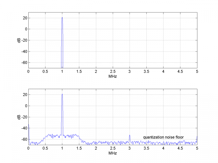
Figure 1. ADC with band-limited Gaussian jitter on sample clock and sinusoidal input.
Top: Spectrum of input signal Bottom: Spectrum of output signal
Nadc= N/2; psd(y,Nadc/8,fs_adc/1e6,flattopwin(Nadc/8))
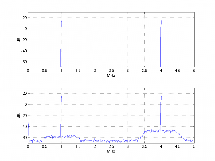
Figure 2. ADC with band-limited Gaussian jitter on sample clock and dual sinusoidal input.
Top: Spectrum of input signal Bottom: Spectrum of output signal
Example 2. Wideband Gaussian jitter
Figures 3 and 4 show the spectra for a sine input to the ADC at 4 Mhz. Both have the same standard deviation of the sample clock jitter to start, but in Figure 3, the jitter is filtered, while it is not filtered in Figure 4 (wideband jitter). The wideband jitter is generated as follows, using the same standard deviation as example 1:
    A= 1e-9;                % s jitter std. deviation
    u= A*randn(1,N);        % AWGN sequence
    dt= u;                  % s jitter of sample clock
We might expect the noise levels near 4 MHz to be the same, but the noise of the wideband jitter case is about 3 dB higher. The reason is that when adc_jitter downsamples the signal by 2, the wideband noise between fs/2 and fs is aliased into the 0 to fs/2 band. We can call this phenomenon a “feature” of adc_jitter, rather than a bug, because it occurs in real-world ADC’s as well. In fact, the noise energy of the sample clock can alias multiple times, since the bandwidth of the sample clock path is normally several times the sample frequency. Unfortunately, the user does not typically know this bandwidth.
If the wideband noise floor is too high, it can harm the ADC’s SNR more than the close-in phase noise. However, low-pass filtering the sample clock is not a cure-all; if the edge is too slow, jitter can be added due to ground noise being transferred to the clock. See [1] for a more detailed discussion.
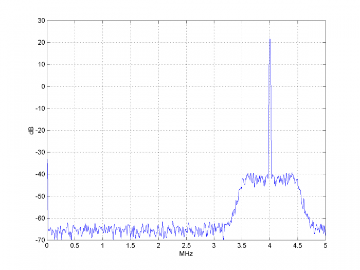
Figure 3. Spectrum of ADC output with band-limited Gaussian jitter on sample clock
and sinusoidal input at 4 MHz.
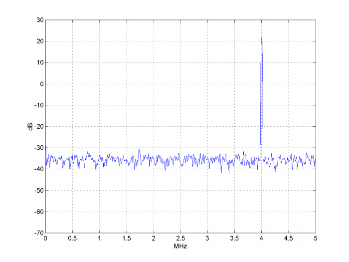
Figure 4. Spectrum of ADC output with wideband Gaussian jitter on sample clock
and sinusoidal input at 4 MHz.
Here’s another peculiar effect of wideband jitter. As we have seen, the spectral noise due to sample clock jitter depends on the frequency of the input signal. Consider an example shown in Figure 5 with wideband Gaussian noise on the sample clock. There are noiseless input sinewaves at 1 MHz and 2.3 MHz, and the signal at 2.3 MHz is 20 dB lower than the signal at 1 MHz. If we move the larger signal to 4 MHz, the noise floor rises by 12 dB (as in Example 1). So the “victim” signal at 2.3 MHz sees its SNR degraded by 12 dB, just due to the new frequency of the larger signal.
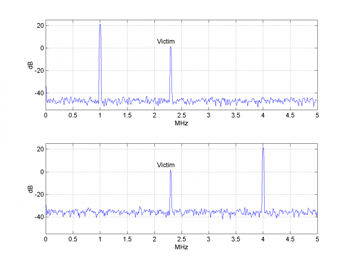
Figure 5. ADC output spectra for two frequencies of input aggressor signal.
Top: Aggressor signal at 1 MHz. Bottom: Aggressor signal at 4 MHz.
Example 3. Close-in Phase Noise
In this example, we model sample clock close-in phase noise by shaping Gaussian noise to resemble a real-world clock source [2]. The noise has a flat region up to almost 10 kHz, followed by frequency ranges with -12 dB/octave and -6 dB/octave slope, followed by flat noise. We achieve this by synthesizing a filter with the desired response and using it to filter Gaussian noise. A Matlab function to synthesize the filter is listed in Appendix A.
As in the earlier examples, I started out using parabolic interpolation to model the ADC jitter, but the resulting jitter at the ADC output was typically about 7% less than the sample clock jitter. I switched to cubic interpolation [3, 4] and got more accurate results. The Matlab function adc_jitter_cubic is listed in Appendix B (The parabolic interpolation version is listed in the appendix of Part 1). Note that the cubic interpolator frequency response for mu= 0.5 is about 1 dB down at fs/4.
The ADC input is a noiseless sinewave.We define the various simulation parameters as in Example 1, noting that input sinewave frequency f0= 3 MHz and the number of samples N is 2^17 = 131,072.
    randn('state',3)                 % initial state of RN generator
    fs_adc= 10E6;                    % Hz ADC sample rate
    f0 = 3E6;                        % ADC input sinewave frequency
    fs= 2*fs_adc;                    % Hz simulation sample rate
    Ts= 1/fs;
    N= 2^17;
    n= 0:N-1;
    x= sin(2*pi*f0*n*Ts);            % adc input
Next we define the noise shaping filter, using three frequencies to determine the regions of different slope. Then we filter the Gaussian sequence and call the function adc_jitter_cubic. We quantize the ADC output to 10 bits.
    f1= 10000; f2= 100000; f3= 1e6;         % Hz filter breakpoints
    [b,a]= noise_filter(f1,f2,f3,fs);
    A= 9e-9;                                % s jitter sigma before noise filter
    u= A*randn(1,N);
    dt= filter(b,a,u);                      % s jitter of sample clock
    dsample= dt/Ts;                         %   jitter in samples
    y= adc_jitter_cubic(x,dsample);         %  ADC jitter function (cubic interp)
    nbits= 10;                            % ADC number of bits (ideal quantization)
    y= floor(2^(nbits-1)*y)/2^(nbits-1);    % quantize to nbits
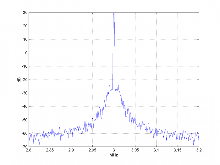
The resulting spectrum at the ADC output is shown in Figure 6, which has a frequency span of 400 kHz. For an ADC output sequence of length 216, we employed spectrum averaging with a psd of length of 216/4 = 16,384 samples. For our ADC sample frequency of 10 MHz, this gives a frequency resolution of roughly 1 kHz using a flat-top window. Had we used a sample frequency of 100 MHz, the frequency resolution would have been very coarse at about 10 kHz. This shows the challenge of modeling close-in phase noise in the frequency domain: the signal of interest has bandwidth much less than the sample rate. So we need many samples to get the desired frequency resolution.
Now let’s compare the jitter on the ADC output signal to the sample clock jitter: they should be approximately equal. To do this, we have to phase-demodulate the signal. The code to perform demodulation is listed in Appendix C. We call the demodulator output ϕd. The time jitter is:
$$\Delta t= \frac{\phi_d}{2\pi}T_0$$
$$ \quad = \frac{\phi_d}{2\pi f_0}$$
The jitter on the sample clock and on the ADC output signal are plotted as histograms in Figure 7. We can also compare the rms jitter of the sample clock and ADC output. RMS jitter is:
$$ \Delta t_{rms}= \left( \frac{\sum(\Delta t)^2}{N} \right)^{1/2}$$
Here are the Matlab calculations. The rms output jitter is only 1.2% away from the rms sample clock jitter:
 dt_ps_rms= sqrt(sum(dt_ps.^2)/N)                   % ps rms jitter of sample clock
 jitter_ps_rms= sqrt(sum(jitter_ps.^2)/length(jitter_ps)) % ps rms jitter of output

 dt_ps_rms =276.7063
 jitter_ps_rms = 280.0680

Figure 6. Spectrum of ADC output for sample clock with shaped Gaussian noise.
Nadc= N/2; psd(y,Nadc/4,fs_adc/1e6,flattopwin(Nadc/4))
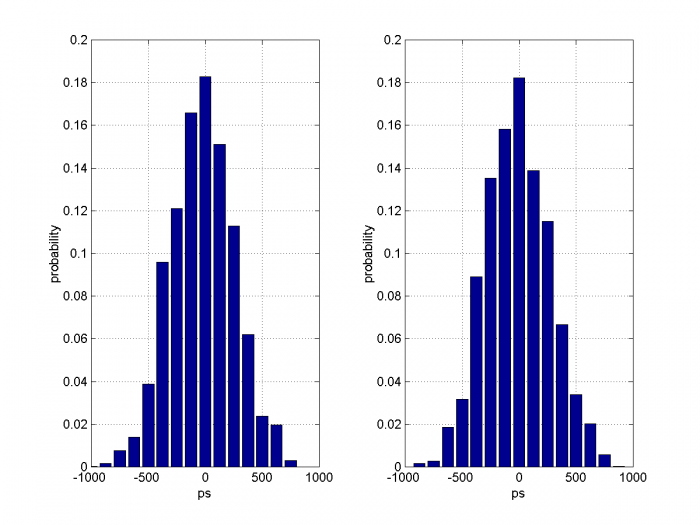
Figure 7. Jitter Histograms for shaped Gaussian noise on sample clock
Left: Jitter of sample clock. Right: Jitter on sinewave at ADC output, f0 = 3 MHz.
References
1. Brannon, Brad, “Sampled Systems and the Effects of Clock Phase Noise and Jitter”, Analog Devices Application Note AN-756, 2004
http://www.analog.com/media/en/technical-documentation/application-notes/AN-756.pdf
2. Goldberg, Bar-Giora, “Phase Noise Theory and Measurements: A Short Review”, Microwave Journal, Jan 1 2000. https://www.google.com/search?q=%2C+Phase+Noise+Theory+and+Measurements%3A+A+Short+Review&oq=%2C+Phase+Noise+Theory+and+Measurements%3A+A+Short+Review&aqs=chrome..69i57.4669j0j8&sourceid=chrome&ie=UTF-8
3. Erup, Lars; Gardner, Floyd M. and Harris, Robert A., “Interpolation in Digital Modems – Part II: Implementation and Performance”, IEEE Transactions on Communications, Vol 41, No. 6, June 1993.
4. Rice, Michael, Digital Communications, a Discrete-Time Approach, Pearson Prentice Hall, 2009, section 8.4.2.
Neil Robertson April, 2018 revised: 4/24/18, 3/30/19
Appendix A Matlab Function noise_filter
This function synthesizes a noise-shaping filter as a cascade of a 2nd order Butterworth lowpass and two proportional + derivative (PD) filters. The function’s inputs are sample rate and three frequencies that set the corner frequencies of the constituent filters. For widely spaced frequencies, the approximate slope of the filter response is:
- flat to f1
- -12 dB/octave between f1 and f2
- -6 dB/octave between f2 and f3
- flat above f3
Each PD filter has flat response from dc to just below the corner frequency f2 or f3, then the response rises at +6 dB/octave. H(z) is given by:
$$ H(z)= b_0+b_1z^{-1}$$
where, for example, to achieve corner frequency of approximately f2, b0 and b1 are:
$$ b_0= \frac{f_s}{2\pi f_2}$$$$ b_1= 1- \frac{f_s}{2\pi f_2}$$
The overall filter response used in Example 3 is shown in Figure A.1 vs. a log frequency scale.
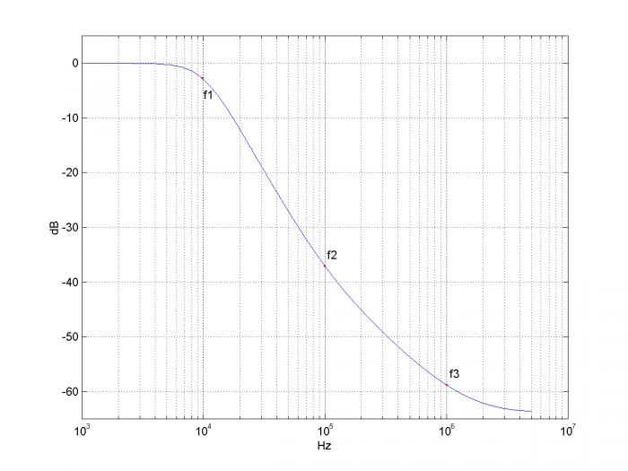
Figure A.1 Noise shaping filter response for f1 = 10 kHz, f2= 100 kHz, f3= 1 MHz, fs= 10 MHz
    %[b,a]= noise_filter(f1,f2,f3,fs)   3/6/18 nr
    %
    % find coeffs of three-filter cascade for noise shaping:
    % 2nd order LP, plus two Proportional-Derivative (PD)
    % f1 = corner of LP, Hz
    % f2= corner of 1st PD filter, Hz
    % f3= corner of 2nd PD filter, Hz
    % fs= sample frequency, Hz
    % for widely spaced frequencies, the approximate slopes are:
    %  -12 dB/octave between f1 and f2
    %  -6 dB/octave between f2 and f3
    %   flat above f3
    %
    function [b,a]= noise_filter(f1,f2,f3,fs);
    % LPF  Use impulse invariant design to avoid null at fs/2.
    w1= 2*pi*f1;
    num= 1;
    den= [1/w1.^2 sqrt(2)/w1 1];  % s-domain 2nd order Butterworth. [1 sqrt(2) 1]
    [b,a]= impinvar(num,den,fs);
    % PD filter 1
    w2= 2*pi*f2;
    d0= fs/w2;
    d1= 1 - d0;                % FIR PD
    d= [d0 d1];
    % PD filter 2
    w3= 2*pi*f3;
    e0= fs/w3;
    e1= 1 - e0;
    e= [e0 e1];                % FIR PD
    b= conv(b,conv(d,e));      % cascade 3 filters(only 1st filter has denom)
Appendix B. Matlab Function adc_jitter_cubic
The function adc_jitter presented in Part 1 used parabolic interpolation. This version uses cubic interpolation. Figure B1 shows the frequency response of the cubic interpolator for mu= 0.5. Because the output is downsampled by two, only the frequency range from 0 to fs/4 is used.
    %function y= adc_jitter_cubic(x,dsample)  4/21/18  Neil Robertson
    % Model ADC with jitter on sample clock, computing jittered samples by
    % cubic interpolation.
    % Add jitter to input signal x, then downsample by 2.
    %
    % x            input signal vector
    % dsample      input jitter vector, jitter in samples
    % y            output signal vector with jitter, sample freq = 1/2 of input fs
    %
    function y= adc_jitter_cubic(x,dsample)
    if length(x)~=length(dsample)
        error('x and dsample must be of equal length')
    end
    N= length(x);
    V= x;
    % find jittered samples using cubic interpolation
    mu= 0.5 + dsample;            % mu = 0.5 +/- jitter
    % Farrow coefficients
    b1= [-1 6 -3 -2]/6;
    b2= [0 1 -2 1]/2;
    b3= [1 -3 3 -1]/6;
    u= zeros(1,N);
    for n= 4:N;
        Vreg= V(n:-1:n-3);       % reg holding 4 samples of V, current sample first
        u(n)= Vreg(3) +...
        mu(n)*( sum(b1.*Vreg) + mu(n)*(sum(b2.*Vreg) + mu(n)*sum(b3.*Vreg)));
    end
    y= u(1:2:end);              % downsample by 2
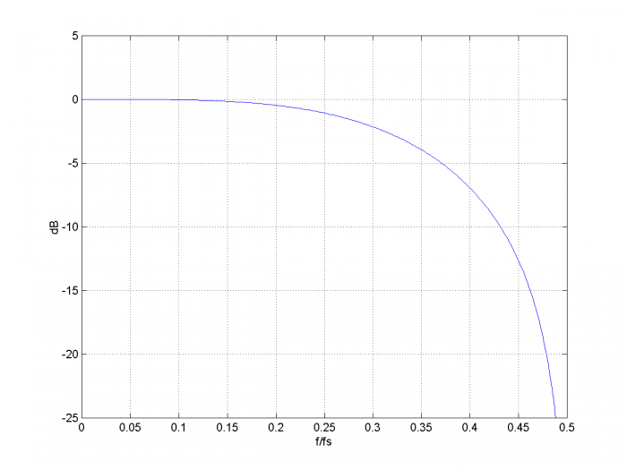
Figure B.1 Cubic Interpolator frequency response for mu= 0.5.
Appendix C. Matlab Code to Demodulate Phase of ADC Output
Here is the code used to demodulate the ADC output in Example 3 and plot the jitter histograms in Figure 7.
    % demodulate ADC output y
    Ts_adc= 1/fs_adc;
    n= 0:Nadc-1;
    LO= exp(-j*2*pi*f0*n*Ts_adc);            % complex local oscillator at f0
    d= LO.*y;                                % complex output of mixer
    fc= .5E6;
    [b,a]= butter(5,2*fc/fs_adc);            % demodulator LPF coeffs
    z= filter(b,a,d);                        % perform LP filtering
    I= 2*real(z(65:end));
    Q= 2*imag(z(65:end));
    phi_d= atan(Q./I);                       % demodulated phase
    mean= sum(phi_d)/length(phi_d);          % mean phase
    phi_d= phi_d - mean;                     % center phase at 0 radians
    ps= -1000:125:1000;                      % ps histogram bins
    % plot sample clock jitter dt_ps as a histogram
    [m,ps]= hist(dt_ps,ps);
    p= m/sum(m);                            % probability of each bin
    subplot(121),bar(ps,p),grid
    xlabel('ps'),ylabel('probability'), axis([-1000 1000 0 .2])
    % plot ADC output jitter (jitter_ps) as a histogram
    jitter_ps= 1E12* phi_d/(2*pi*f0);
    [m,ps]= hist(jitter_ps,ps);
    p= m/sum(m);                            % probability of each bin
    subplot(122),bar(ps,p),grid
    xlabel('ps'),ylabel('probability'),axis([-1000 1000 0 .2])
- Comments
- Write a Comment Select to add a comment
Thank you for sharing these wonderful articles, thy are very informative! I was curious if you already know the answer to this question: Given that a delta-sigma ADC will reshape quantization noise, do you know if the same principal can be applied to reshaping the noise from clock jitter? My gut instinct is that it would, but I’m not sure I could prove it analytically, or even how to go about modeling it

Dszabo,
I'm glad you find my posts helpful. I don't know the answer to your question. (I'm inclined to think that a delta-sigma ADC's sample clock noise would affect the input signal the same as a regular ADC). Maybe someone else will comment.
regards,
Neil
Dear Mr. NeiRober
At first, thanks deeply for your sharing paper.
After read your paper, I step to step test it on Matlab.
Some issues which made me wondered.
Because I want to get some advises from you and for convenient communication(because some time the picture or code need be added). Could you share your personal email?
If my request brings to you inconvenient, please forgive me!
Hi,
If you want to email me, click on the email icon underneath "About Neil Robertson".
Neil
Today I fixed a few small errors in this post: I replaced "jitter per sample" with "jitter in samples" in several places. I also corrected the pdf version.
Neil
Hi Neil,
Thanks for the excellent post!
I was about to drill into the interpolation stuff, but the first glance over the code makes me wonder if the third-order is missing from the expression:
mu(n)*( sum(b1.*Vreg) + mu(n)*(sum(b2.*Vreg) + mu(n)*sum(b3.*Vreg)));
should it be:
mu(n)*( sum(b1.*Vreg) + mu(n)*(sum(b2.*Vreg) + mu(n)^2 *sum(b3.*Vreg)));
?
Thanks!
George
George,
The formula for u could be evaluated as a standard 3rd order polynomial. However, for efficiency, I used Horner's method instead. If you expand the formula (keeping track of nested parenthesis), you will find that it is cubic in mu.
A description of Horner's method is given in section 13.26 of Richard Lyons book, "Understanding Digital Signal Processing", 3rd ed.
regards,
Neil
Hi Neil.
Thank you so much for all this information! Amazing and it is helping me a lot! Just one little doubt: do you know if there is an equation that I can measure (in theory) the level of the noise floor (wideband Gaussian Jitter)? I ask you this question because I changed some frequencies and I am not sure about my results. I would like to compare the theory with my noise floor level results (the wideband gaussian one.
Thank you so much!
Andre,
I don't have an equation for the absolute noise floor for wideband Gaussian jitter. However, the -20*log10(fs/f0) relationship of Equation 4 in Part 1 holds. For example, in Figure 5 of Part 2, the noise floor rises 12 dB when the aggressor signal frequency is moved from 1 MHz to 4 MHz (fs constant at 10 MHz).
Note the spectral folding of wideband Gaussian noise is discussed in reference 1 of Part 2.
regards,
Neil
To post reply to a comment, click on the 'reply' button attached to each comment. To post a new comment (not a reply to a comment) check out the 'Write a Comment' tab at the top of the comments.
Please login (on the right) if you already have an account on this platform.
Otherwise, please use this form to register (free) an join one of the largest online community for Electrical/Embedded/DSP/FPGA/ML engineers:


