


Simulink-Simulation of SSB demodulation
Simulink-Simulation of SSB demodulation or modulation from the article “Understanding the ‘Phasing Method’ of Single Sideband Demodulation” by Richard Lyons
Josef Hoffmann
The article “Understanding the ‘Phasing Method’ of Single Sideband Demodulation” by Richard Lyons is a very good description of this topic. The block representation from the figures are clear and easy to understand. They are predestined for a simulation in Simulink. The simulation can help clarify many additional questions and enable further creative investigations. The theory and explanations from the mentioned article are not repeated here. If necessary, some explanations are added to clarify the simulation.
Simulation of the simple demodulation of the SSB signals
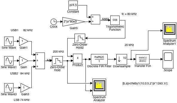
Fig. 1 shows the Simulink model for the demodulation of a USB signal assuming that only this signal exists and no LSB signal with the same carrier is present. In this case, it is sufficient in the receiver to multiply the USB signal with a synchronous carrier.
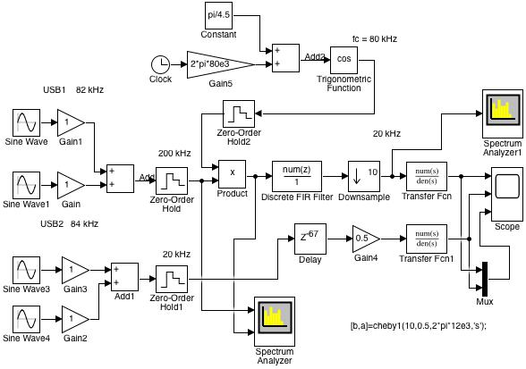
Two sinusoidal signals with a frequency of 82 kHz and 84 kHz with different amplitudes equal to 1 and 5 are applied as input signals. For a carrier frequency equal to $ f_c = $ 80 kHz, these signals represent two signals in the USB range. They are converted into digital signals with the ‘Zero-Order Hold’ block and a sampling frequency of 200 kHz.
With the ‘Product’ block, the digital input signals are multiplied by the carrier frequency generated in the receiver. This carrier frequency is generated in the upper part of the model. Here one can set the frequency and also the zero phase. In this way one can examine the influence of a frequency and phase deviation on the demodulated signal.
The product is digitally low-pass filtered with the ‘Discrete FIR Filter’ block and further decimated by a factor of 10. The 128 order filter has a relative passband of 0,1 or absolute passband of 10 kHz.
This gives the digital demodulated signal with a sampling frequency of 200/10 = 20 kHz, the power spectrum of which is shown with the ‘Spectrum Analyzer1’ block. The digital demodulated signal after the ‘Downsample’ is converted with an analog filter into an analog signal with the help of the ‘Transfer Fcn’ block. Before the simulation can be started, this filter must be initialized in the MATLAB workspace:
[b,a] = cheby1(10,0.5,2*pi*12e3,'s');
It is a Chebyshev low-pass filter type ‘cheby1’ of order 10 with ripple in the passband equal to 0,5 dB and passband equal to 12 kHz.
In the lower part of the model, a baseband signal is formed that can serve as a model of the modulation signal. The one signal with the frequency 2 kHz would yield the USB signal of 82 kHz and the second signal with the frequency 4 kHz would yield the USB signal with 84 kHz. Fig. 2 shows the spectrum that is displayed on the ‘Spectrum Analyzer’ block which has two entries.
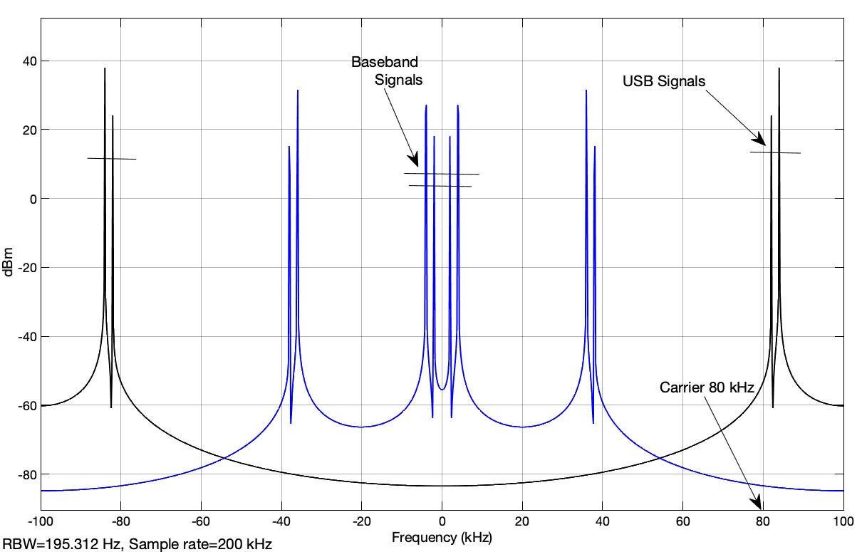
The first input of the ‘Spectrum Analyzer’ shows the spectrum of the input signals with frequencies of 82 kHz and 84 kHz which relative to the carrier of 80 kHz form the USB signals of the simulation. With a sampling frequency fs = 200 kHz, the frequency range from -fs / 2 = -100 kHz to fs / 2 = 100 kHz is displayed.
The second spectrum for the signals at the second input of the ‘Spectrum Analyzer’ shows the spectrum after multiplication with the generated carrier at the receiver in the ‘Product’ block.
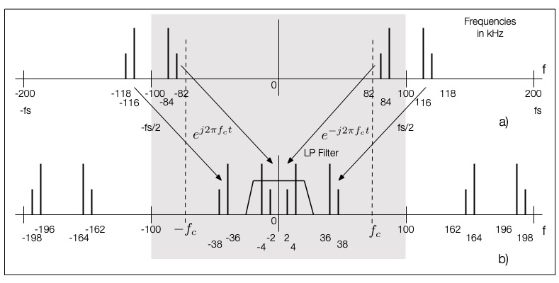
Fig. 3 shows a sketch to explain the spectrum from Fig. 2. The area shown on the ‘Spectrum Analyzer’ block is blackened. If a signal $ s (t) $ with a Fourier transform $ S (f) $ (as a spectrum) is multiplied with a function
$$ cos(2 \pi f_c t)=\frac{1}{2}(e^{2\pi f_c t} + e^{-2\pi f_c t}) $$
it will give the following shifted spectrum [6]:
$$ \mathcal{F}\{s(t)cos(2 \pi f_c t) \}=\frac{1}{2}\big(S(f-f_c) + S(f+f_c)\big) $$
The first term $ S(f-f_c) $ represents the shift to the right of the spectral lines with negative frequencies. The second term shows how the spectral lines with positive frequencies shift to the left. The additional lines from Fig. 3 in the area $ f \geq f_s / 2 $ or $ f \leq -f_s / 2 $ arise because of the symmetry of the DFT (‘Discrete Fourier Transformation’) for discrete signals [6].
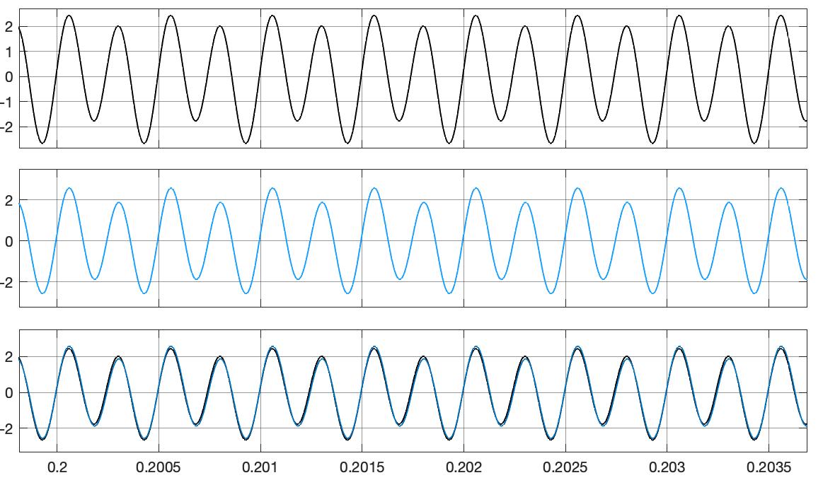
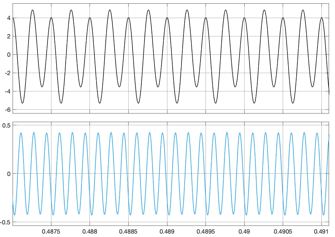
Three signals are displayed on the ‘Scope’ block, as shown in Fig. 4. The demodulated signal is shown at the top, the artificially generated modulation signal is shown below and finally both are shown superimposed at the bottom. Almost the same signals are obtained when a correct carrier frequency of 80 kHz is set in the ‘Gain5’ block and a zero phase of the carrier equal to $ \pi/4.5 $ is initialized through trials in the ‘Constant’ block.
The shown demodulation of the USB signal by simple multiplication with the carrier $ cos(2\pi f_c t) $ can be used if one knows that there is no LSB signal with the same carrier. What happens when such an additional LSB signal is present will be examined with the model ‘SSB02.slx’. In addition to the previous signals of frequencies 82 kHz and 84 kHz, a signal of frequency 74 kHz is added to the input, as shown in Fig. 5. For a carrier with a frequency of 80 kHz, this signal represents an LSB signal.
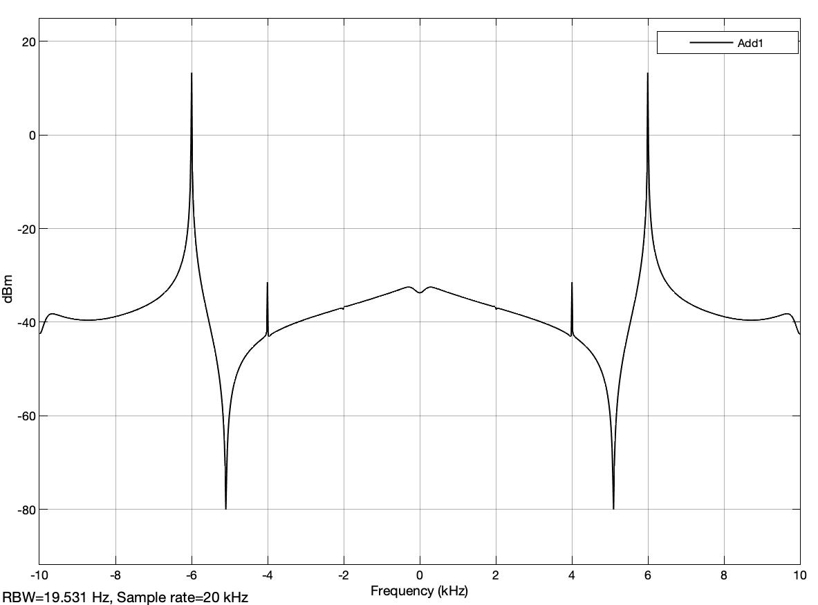
The spectrum of the input signals and the spectrum after the product with the carrier generated at the receiver, as displayed on the ‘Spectrum Analyzer’ block, are shown in Fig. 6.
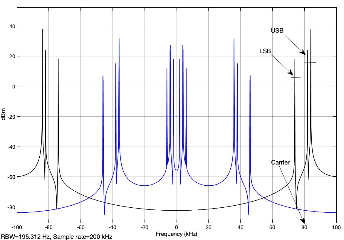
To the right of the carrier with the frequency of 80 kHz are two lines of the spectrum for the signals with frequencies 82 kHz and 84 kHz which form the USB signals. To the left of the carrier the signal of 74 kHz can be seen as the LSB signal.
The product with the carrier gives the second spectrum from Fig. 6, with the shifts in the baseband. One can see, these mixed products can no longer separate the two signals of 2 kHz and 4 kHz that correspond to the USB signals and the signal of 6 kHz that corresponds to the LSB signal.
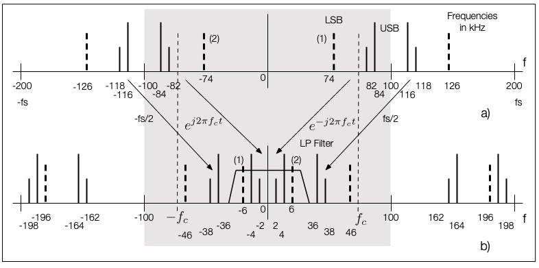
The sketch in Fig. 7 explains the different line spectra from Fig. 6. The sketch is an extension of the sketch from Fig. 3. The spectral line for the LSB signal with 74 kHz is added with a dashed line. The line at 74 kHz is shifted to -6 kHz after multiplication with the carrier of the frequency 80 kHz and vice versa the line at -74 kHz is shifted to 6 kHz. The remaining lines of the periodic spectrum of the digital signals are also shifted. The demodulated signals, which correspond to the USB and LSB signals, cannot be separated from the lines shown in the baseband.
Simulation of the ‘Phasing Method’ for demodulating SSB signals
The demodulation according to the block diagram from Figure 13 of the article “Understanding the ‘Phasing Method’ of Single Sideband Demodulation” by Richard Lyons , which is shown here again,
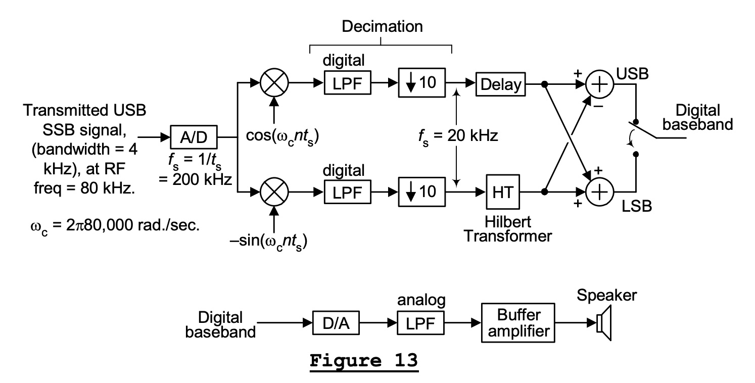
form the basis of this simulation. The reason for this arrangement is shown in the aforementioned article based on the real and imaginary parts of the spectrum of the signals. The mode of operation of this arrangement is explained here with the aid of the magnitudes and phases of the spectra.
Fig. 9 shows a sketch which explains the spectra of the signals according to the arrangement from Fig. 8. A time-continuous signal is assumed. Fig. 9a shows the spectra of the signals in the bandpass range. The amount of the spectrum of the LSB signal is highlighted in black. With slightly thicker lines, the phases of the spectra are shown with the known symmetry for positive and negative frequencies.
The multiplication of the input signals with the cosine function of the carrier $ cos(2\pi f_c t) $ leads to the shifts shown in Fig. 9b and Fig. 9c. One must imagine these spectra $ S_ {11} (f), S_ {12} (f) $ superimposed, as described in the previous section.
The same input signals multiplied by the sine function $ -sin(2\pi f_c t) $ result in the spectra from Fig. 9d and Fig. 9e, which one also has to imagine superimposed.
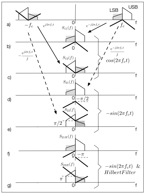
Because of the division with $ j $ in the complex representation of the sine function
$$ -sin (2 \pi f_c t) = \frac{1}{2j} (- e ^ {2 \pi f_c t} + e ^ {- 2 \pi f_c t}) $$
the phases in Fig. 9d are shifted with $ - \pi/ 2 $. Similar are the phases from Fig. 9e once shifted with $ - \pi $ because of the minus sign and again shifted with $ - \pi/ 2 $ because of the $ j $ in the denominator of the complex representation of the sine function.
When the input signals are multiplied by $ cos (2 \pi f_c t) $ and $ -sin (2 \pi f_c t) $, mixed products arise also in the vicinity of $ 2f_c $ or $ -2f_c $, which are suppressed with the help of low-pass filters.
The product of the input signals with the sine function with minus sign is low-pass filtered and further with the Hilbert filter transformed. This filter does not change the amount of the spectra, but adds an additional phase of $ - \pi / 2 $ for positive frequencies and a $ \pi / 2 $ phase for negative frequencies, as shown in Fig. 9f and Fig. 9g.
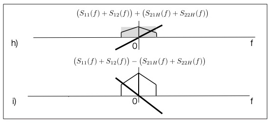
If one now adds the partial spectra from Fig. 9b and Fig. 9c with the partial spectra from Fig. 9f and Fig. 9g, one gets the spectrum from Fig. 10h, which corresponds to the baseband signal of the LSB signal. The components from the LSB signal are in phase and add up and the components from the USB signal are phase-shifted with $ \pi $ and add up to zero.
The difference between the same spectra results in the spectrum from Fig. 10i, which corresponds to the baseband signal of the USB signal. Here, the difference in the components of the same phase for the spectrum from the LSB signals results in zero values. In this form, the demodulation has correctly separated the LSB and USB signals with the same carrier in the passband.
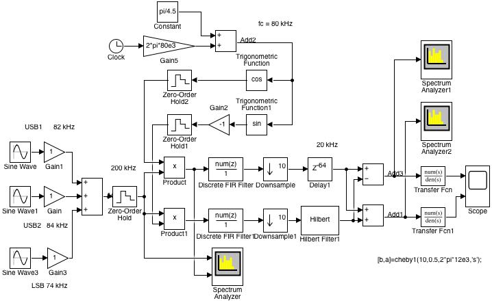
Fig. 11 shows the Simulink model for simulating the demodulation with the ‘Phasing method’. It simulates the arrangement from Fig. 8. Two sinusoidal signals with frequencies 82 kHz and 84 kHz are applied as input signals, which form the USB signals relative to the carrier frequency of 80 kHz. In addition, a signal with a frequency of 74 kHz is applied as an LSB signal. After sampling with a sampling frequency of 200 kHz, these signals are multiplied with $ cos (2 \pi f_c t) $ and $ -sin (2 \pi f_c t) $ in the blocks ‘Product’ and ‘Product1’.
After the low-pass filtering with the blocks ‘Discrete FIR Filter’ and ‘Discrete FIR Filter1’, there is the possibility of reducing the sampling rate from 200 kHz to 20 kHz by decimation with a factor of 10. This decimation is implemented using the ‘Downsample’ and ‘Downsample1’ blocks.
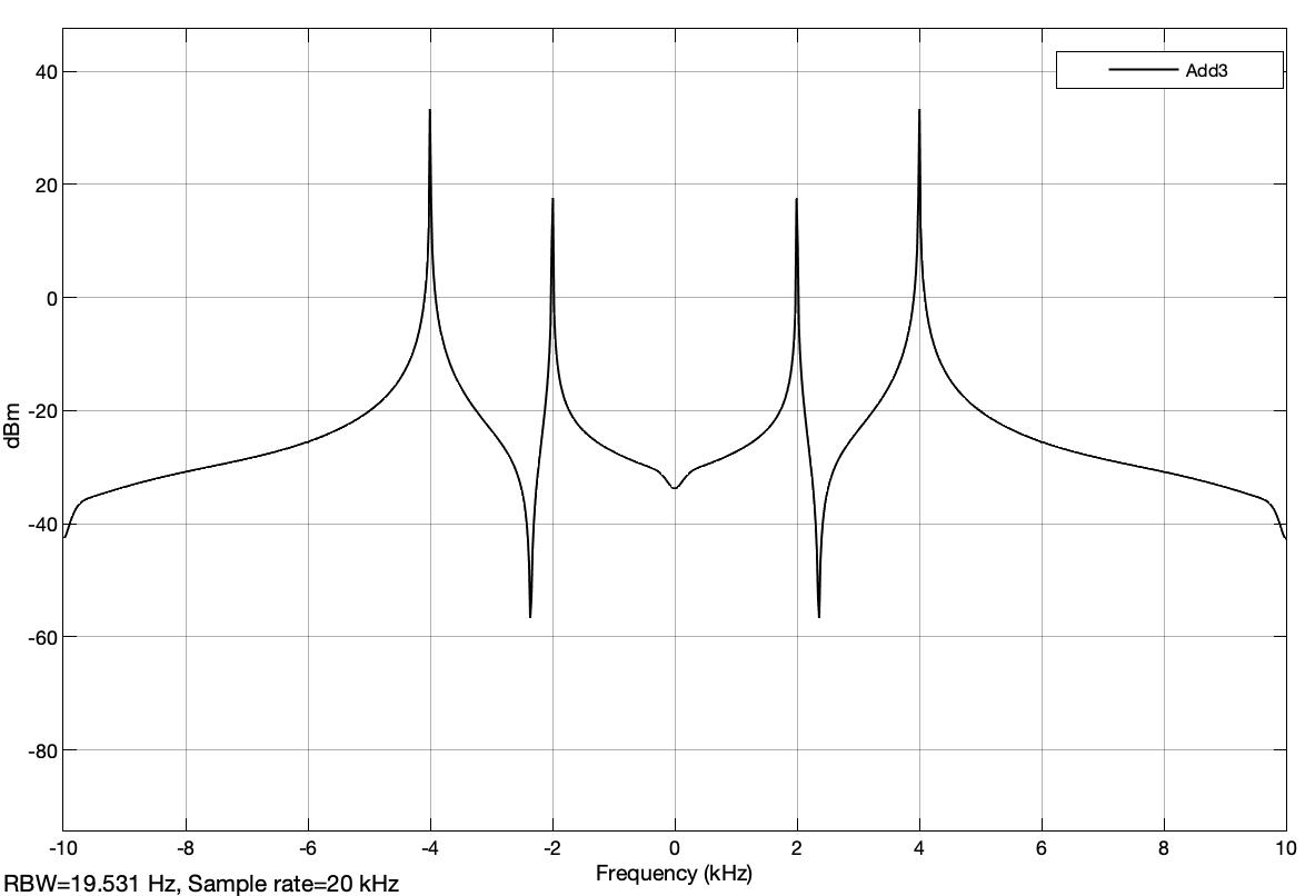
The signal of the lower path is Hilbert transformed with the block ‘Hilbert Filter1’. To align the signals of the two paths, the delay of the Hilbert filter is simulated with the ‘Delay1’ block. The difference between the signals of the two paths results in the demodulated USB signal consisting of a signal with a frequency of 2 kHz and a signal with a frequency of 4 kHz. The sum of the same signals leads to the demodulated LSB signal consisting of a signal with a frequency of 6 kHz.
The spectrum of the demodulated USB signal is displayed with the ‘Spectrum Analyzer1’ block, as shown in Fig. 12. One can see the two components of the frequency 2 kHz and 4 kHz. Similarly, with the ‘Spectrum Analyzer2’ block, the spectrum of the demodulated LSB signal is displayed and shown in Fig. 13. Here one can see the component of the frequency 6 kHz.
The demodulated signals after the analog filters are shown in Fig. 14: on top the demodulated USB signal of the frequency 2 kHz and 4 kHz and below the demodulated LSB signal of the frequency 6 kHz.
Before starting the simulation, the analog filter must be initialized in the MATLAB ‘Workspace’:
[b, a] = cheby1 (10,0.5,2 * pi * 12e3, 's');
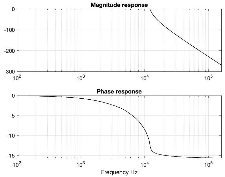
Fig. 15 shows the frequency response of the analog Chebyschev filters. The phase response is not linear and this creates additional distortion. One can also experiment with other filters (e.g. Butterworth filters).
With the ‘Spectrum Analyzer’ block, the spectrum of the input signals and the spectrum of the product with the cosine function of the carrier are displayed showing the same spectra as in Fig. 6.
SSB modulation with ‘Phasing Method’
In the article “Understanding the ‘Phasing Method’ of Single Sideband Demodulation” von Richard Lyons the SSB modulation is also described and in the figure ‘Figure A-1’ understandably explained. A modulation signal in the form of a simple cosine signal was used and the transformations which lead to the SSB signal are very easy to understand.
The same method as with the demodulation is used here to explain the modulation. From the modulation signal m(t) a complex signal ma(t) is defined:
$$ m_a = m (t) + j ~ m_H (t) $$
This complex signal is already one-sided in the baseband and has spectral components only for $ f \geq 0 $ for a later USB bandpass signal or has only spectral components for $ f \leq 0 $ for a later LSB bandpass signal.
Here the signal $ m_H(t) $ is the Hilbert transformation of the modulation signal $ m(t) $ [2]. As already shown in the previous chapter, imagining this transformation using a filter, then this filter has a complex frequency response of the form:
$$ H (f) = -j ~ sign (f) $$The $ sign $ denotes the signum function, which is equal to 1 if the argument is positive and -1 if it is not. The amplitude spectra $ | M(f) | $ and $ | M_H(f) | $ of $ m(t) $ and $ m_H(t) $ are the same, only the phase spectra differ by $ - \pi / 2 $ for $ f> 0 $ and $ \pi / 2 $ for $ f \leq 0 $. As one can see, the Hilbert filter also plays an important role in modulation.
The complex signal $ m_a(t) $ is a mathematical assumption or model consisting of two physically real signals $ m(t) $ and $ m_H(t) $. The complex signal is designed in such a way that a one-sided spectrum is obtained in the baseband. The $ m_a(t) $ signal is also known as the analytical signal [2], and Simulink has a block that generates this signal and provides a mathematical complex output.
Fig. 16 shows how to obtain a one-sided spectrum for this complex signal.
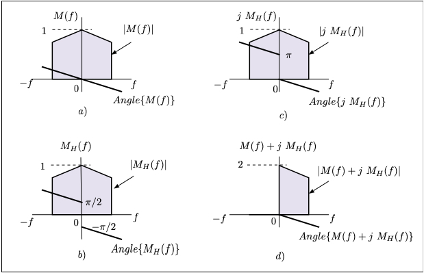
Based on the spectrum of the modulation signal from Fig. 16a, which has the usual symmetry of the Fourier transformation of real signals, the spectrum from Fig. 16b is obtained by the Hilbert filter. One can observe the change in the phase spectrum with $ - \pi / 2 $ for $ f>0 $ and with $ \pi/ 2 $ for $ f \leq 0 $. The output of the Hilbert filter $ m_H(t) $ multiplied by $ j $ gives a spectrum as in Fig. 16c, because to the phase spectrum from Fig. 16b a $ \pi/2 $ phase is added over the entire frequency range.
In the spectrum of the sum $ M (f) + j ~ M_H (f) $, the areas for negative frequencies with $ \pi $ phase are shortened, so that the one-sided spectrum from Fig. 16.d arises. For the other one-sided spectrum, which only has parts for negative frequencies, instead of the sum $ M (f) + j ~ M_H (f) $ the difference $ M (f) - j ~ M_H (f) $ must be formed.
The physically real bandpass signal is formed as follows:
$$ s (t) = m (t) ~ cos (2 \pi f_c t) + m_H (t) ~ sin (2 \pi f_c t) $$
In order to calculate the spectrum of this signal, the signal is expressed in complex:
$$ s (t) = R_e \{ m_a (t) e ^ {j2 \pi f_c t} \} $$
Here $ R_e \{\} $ forms the real part of the complex argument. The Fourier transform $ S (f) $ of this signal is:
$$ S (f) = \int_{- \infty} ^\infty s(t) e ^{- j2 \pi ft} dt = \int_{- \infty}^\infty R_e \{m_a (t) e^{j2 \pi f_c t} \} e ^ {- j2 \pi ft} dt $$
The real part of a complex quantity $ \xi $ can be determined by
$$ R_e \{\xi \} = \frac{1}{2} (\xi + \xi ^ *) $$
where * defines the conjugated complexes. The Fourier transform $ S (f) $ is then:
$$ S(f) = \frac {1} {2} \int_{- \infty} ^ \infty [m_a(t) e^{j2 \pi f_c t} + m_a ^ * (t) e ^ {- j2 \pi f_c t}] e^{- j2 \pi f t} dt = \frac{1}{2} \big[M_a(f-f_c) + M_a ^*(-f-f_c)\big] $$
$ M_a(f) $ is the Fourier transform of the complex signal $ m_a(t) $. The result according to this equation is shown in Fig. 17. The spectrum $ S (f) $ of the real bandpass signal $ s(t) $ is given from a sum of the shifted spectra of the complex signal $ m_a(t) $.
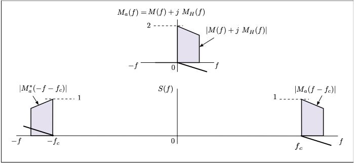
The complex signal is comprised of two real signals $ m (t) $ and $ m_H (t) $, from which a one-sided spectrum can be obtained in the baseband. After the modulation, a real signal $ s (t) $ in the bandpass range is obtained with a spectrum $ S (f) $ that has the well-known symmetry for real signals.
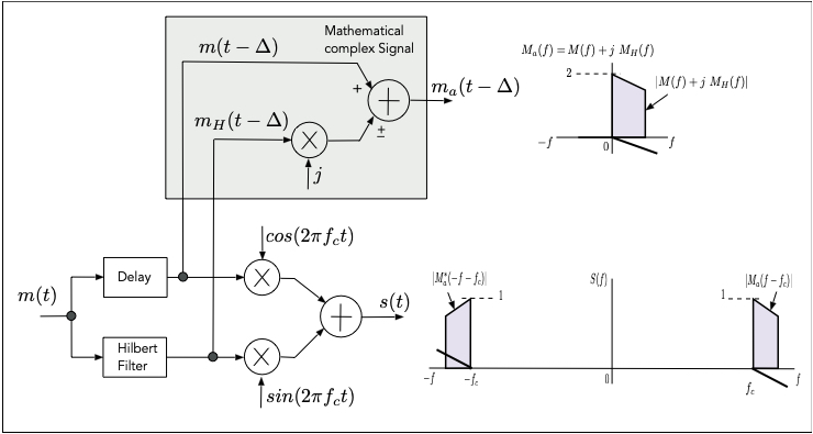
Figure 18 shows the formation of the bandpass signal $ s(t) $ and of the complex signal $ m_a(t)) $. The Hilbert filter implemented digitally, e.g. as an FIR filter, results in a linear phase shift in addition to the function described, which acts as a delay for the signal. In the case of an FIR filter of the order north, this delay is equal to north/2 and must also be provided in the direct path of the signal $ m(t) $ in order to get the signals of the two paths correctly aligned.
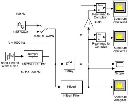
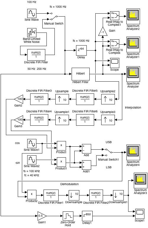
With the Simulink model from Fig. 19 the creation and investigation of the complex signal $ m_a (t) $ is described. The modulation signal $ m(t) $ at the input can be chosen between a cosine-shaped signal of the frequency 100 Hz and a band-limited noise signal with components in the range 50 Hz to 200 Hz.
The Hilbert filter was set with an order equal to 128, so that the delay for the correct alignment of the two signals $ m(t) $ and $ m_H(t) $ was initialized to 64 in the ‘Delay’ block. These two signals can be seen on the ‘Scope’ block. For the cosine input signal the two signals are shown in Fig. 20. One recognizes the phase shift of $ -\pi/ 2 $ between these signals.
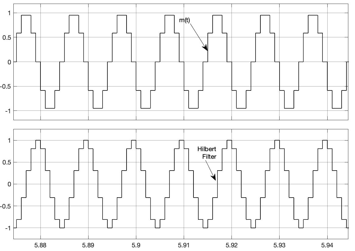
Fig. 21 shows the amount of the spectrum of the signal at the output of the Hilbert filter when the input signal is the cosine-shaped signal of 100 Hz, as displayed with the ‘Spectrum Analyzer’ block. One recognizes the symmetry of the spectrum for real-valued signals. The same amount of spectrum is obtained if the ‘Spectrum Analyzer’ block is connected to the output of the ‘Delay’ block with the $ m(t-\Delta) $ signal. They only differ in the phase spectrum.
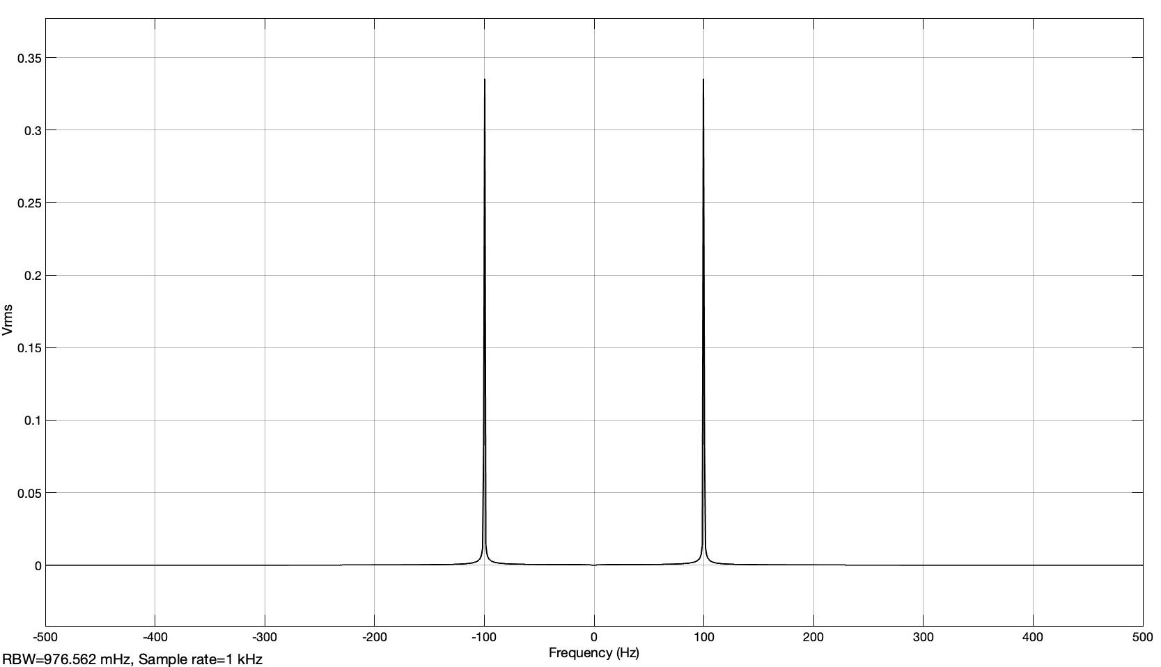
The magnitude of the spectrum of the complex signal is shown with the ‘Spectrum Analyzer1’ block, as displayed in Fig. 22. With the ‘Real-Imag to Complex’ block, a complex signal is formed from the two real signals. The spectrum is now one-sided with a spectral line at 100 Hz.
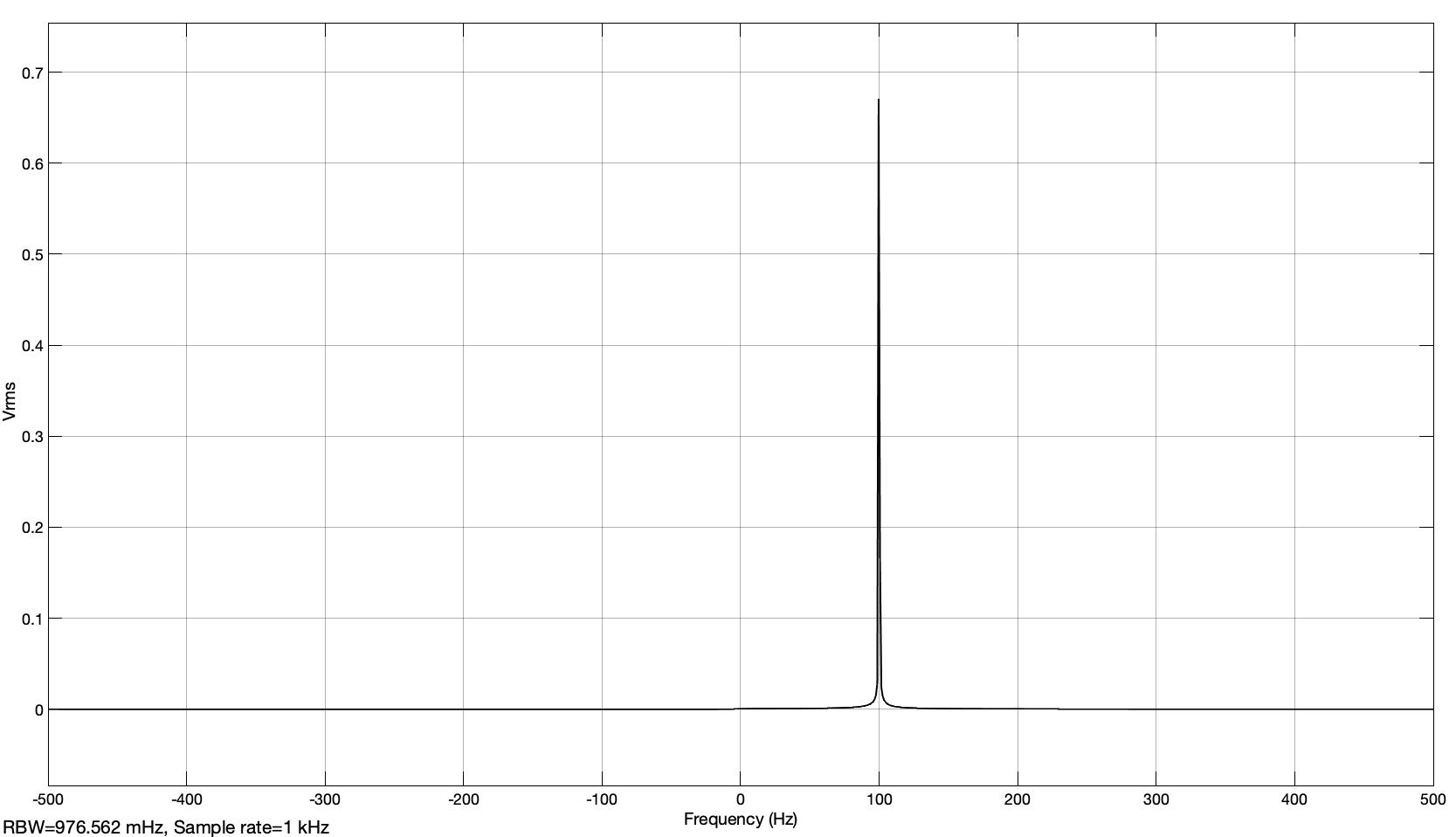
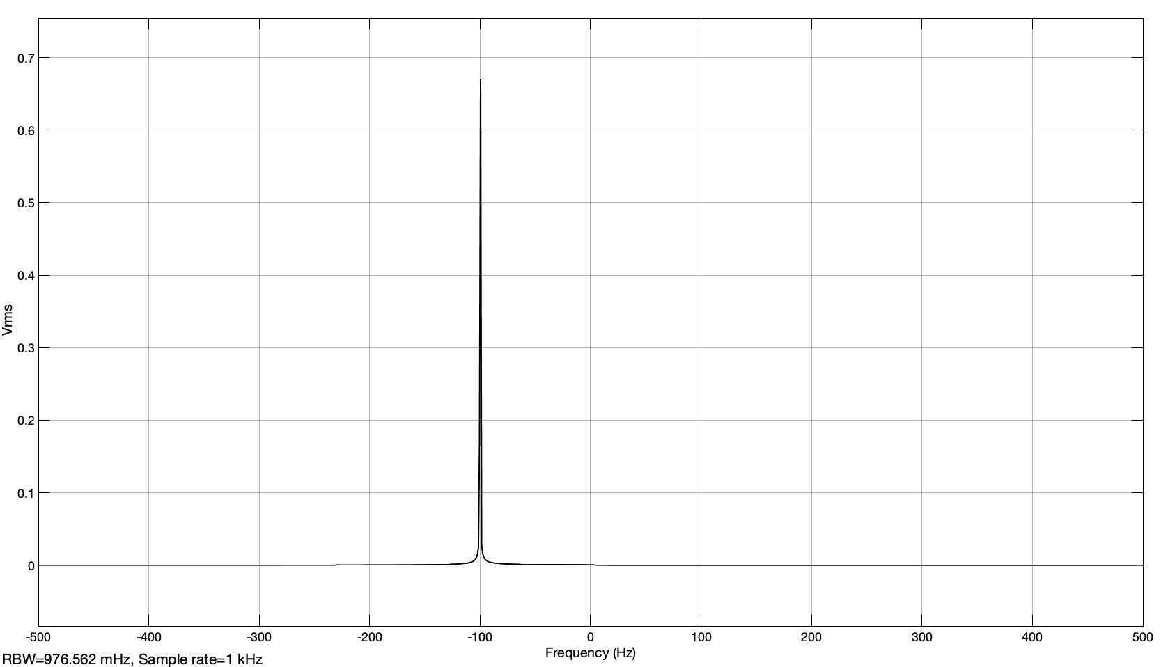
If one gives a negative sign to the imaginary part, then the one-sided amount of the spectrum from Fig. 23 with a spectral line at -100 Hz, as displayed by the ‘Spectrum Analyzer2’ block, is optained. The effective values shown do not quite correspond to the expected values because of ‘leakage’ [2].
The amplitude 1 should give one line of $ 1 /\sqrt(2) = 0.707 ... $ as the effective value and for the two lines trough division by two should give the value $ 0.3536 ... $ which distinguish from the value in Fig. 21. The values from Fig. 22 and Fig. 23 should be $ 1/\sqrt (2) = 0.707 ... $$
With the band-limited noise input, the power spectral density in dBWatt/Hz (which must be initialized at the ‘Spectrum Analyzer’ blocks) is shown in Fig. 24, Fig. 25 and Fig. 26.
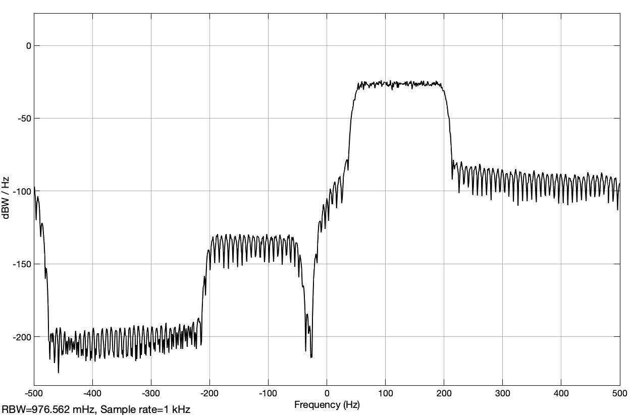
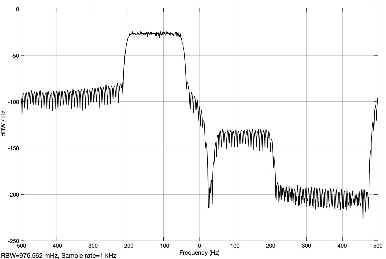
The power spectral density is shown in logarithmic coordinates and a much larger range of values is displayed. The noise source from the ‘Band-Limited White Noise’ block is parameterized in such a way that a variance or power equal to 1 watt is obtained. With a sampling frequency of 1000 Hz, a power spectral density equal to $ 1/1000 $ Watt/Hz is obtained. This results in a power spectral density of $ 10 ~ log_ {10} (1/1000) = -30 $ dBWatt / Hz. This value can be seen roughly in all three representations.
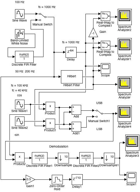
Fig. 27 shows the Simulink model of the SSB modulation with the simple demodulation, which is also present, mentioned before to check the functionality. In the upper part of the model you can see the arrangement from the previous model (analyt_sig_1.slx). In the middle, the modulation is shown with a carrier frequency of 40 kHz at a sampling frequency of 100 kHz.
It is very difficult to simulate a system when there are two sampling frequencies that are very different. In the block presentation of the modulation in Figure A-2 from the mentioned article, a sampling frequency of 12 kHz is for the modulation signal and a sampling frequency of 36 MHz for the carrier are chosen. In each step for the modulation signal there are 36000/12 = 3000 carrier steps. This results in a very slow simulation. Here was a carrier frequency chosen that is not so large relative to the bandwidth of the modulation signal.
In the lower part, the simple demodulation is shown, with which one can check the functionality of the modulation. The required carrier signal is taken from the modulation part. In practice, the receiver knows the carrier’s frequency, but synchronization with the transmitter’s carrier must be implemented separately [5].
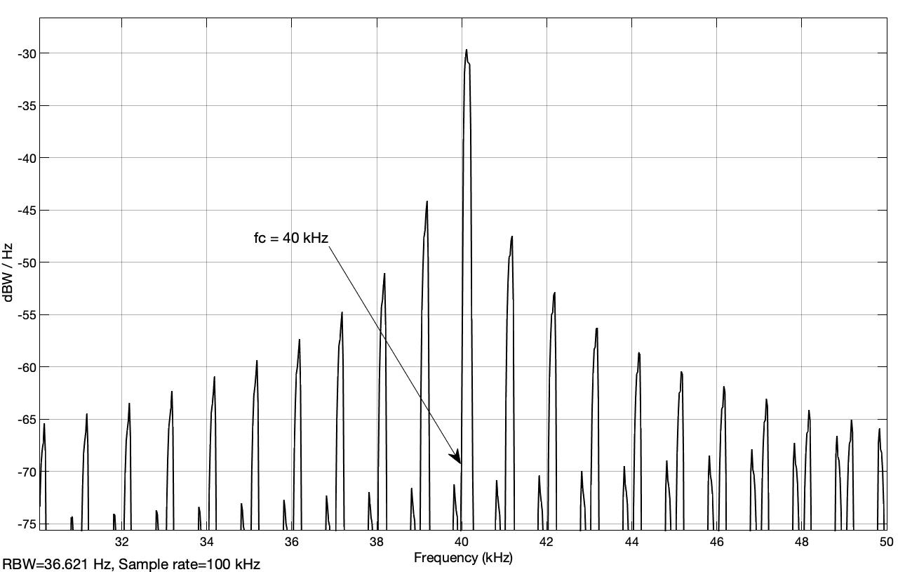
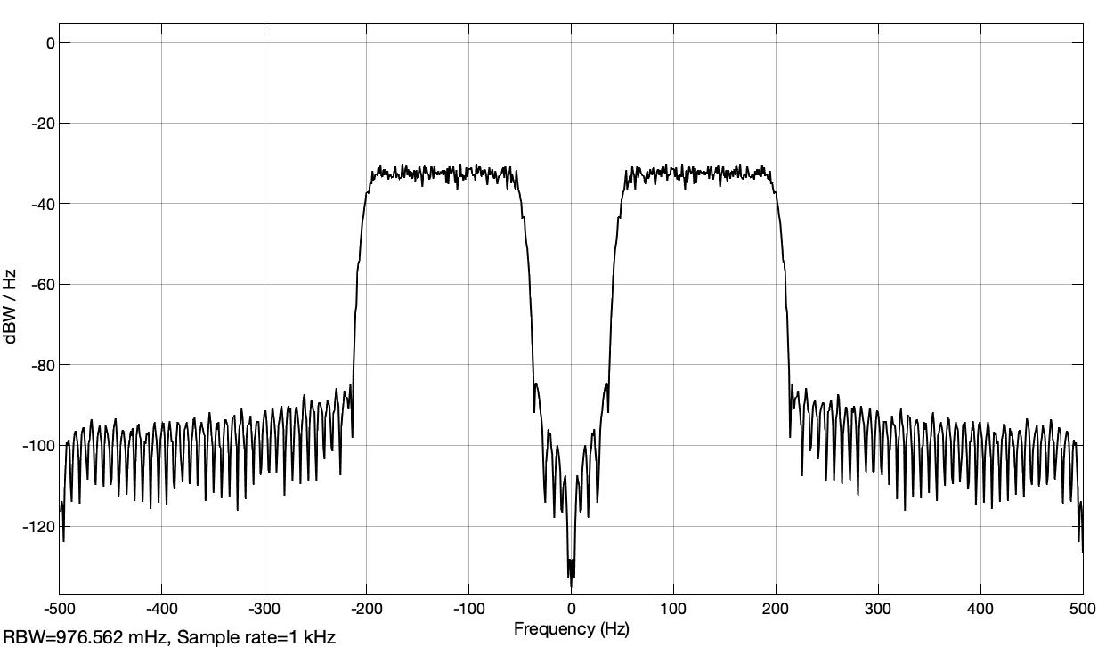
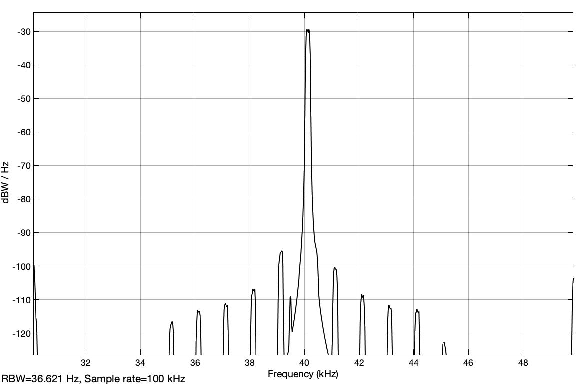
A zoom section of the power spectral density of the USB bandpass signal is shown in Fig. 28, as displayed on the ‘Spectrum Analyzer4’ block. The sidelobes with a spacing of 1 kHz, which is the sampling frequency of the modulation signal, are attenuated with only -15 dBWatt/Hz.
Fig. 29 shows the Simulink model of the modulation, in which the modulation signal is brought to the same sampling frequency of 100 kHz as for the carrier signal using an interpolation with a factor of 100.
The spectral power density of the USB bandpass signal, which is displayed in Fig. 30, shows that the side lobes are much more attenuated with approx. - 60 dBWatt/Hz.
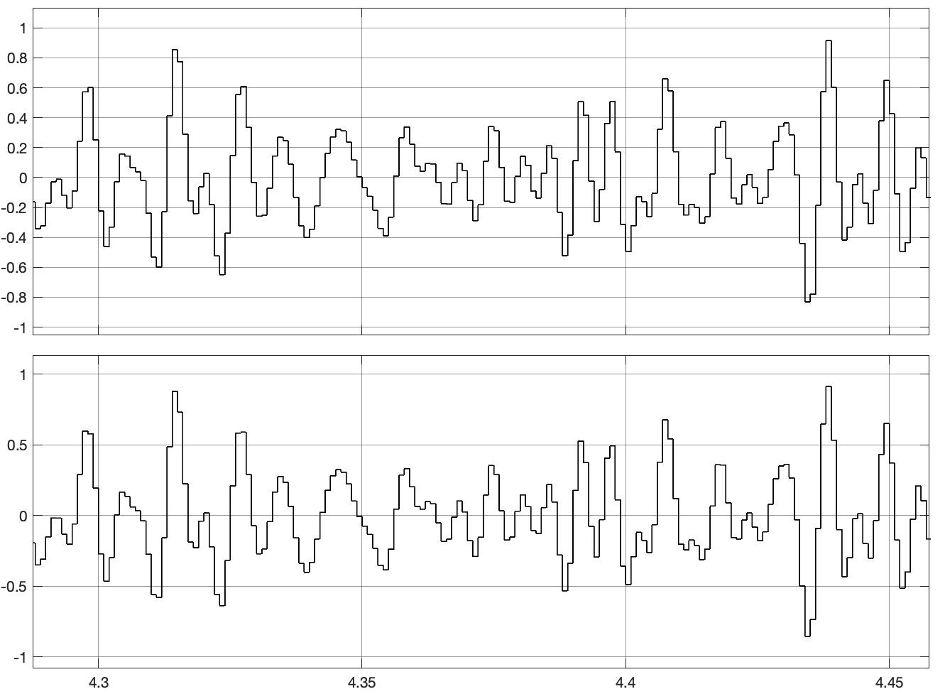
The modulation signal and the demodulated signal shown on the ‘Scope1’ block are now practically the same, as shown in Fig. 31.
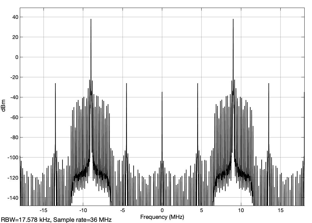
In the block representation from ‘Figure A-2’ of the article “Understanding the ‘Phasing Method’ of Single Sideband Demodulation” von Richard Lyons contains an interpolation of the modulation signal with a factor of 3000. This brings the sampling frequency of 12 kHz of the modulation signal to a sampling frequency of 36 MHz, which is provided for the carrier frequency of 9 MHz.
This modulation is simulated in the Simulink model ‘analyt_sig_4.slx’, which is shown in Fig. 32. The interpolation with factor 3000 is implemented in three stages with factors 15, 25 and 8.
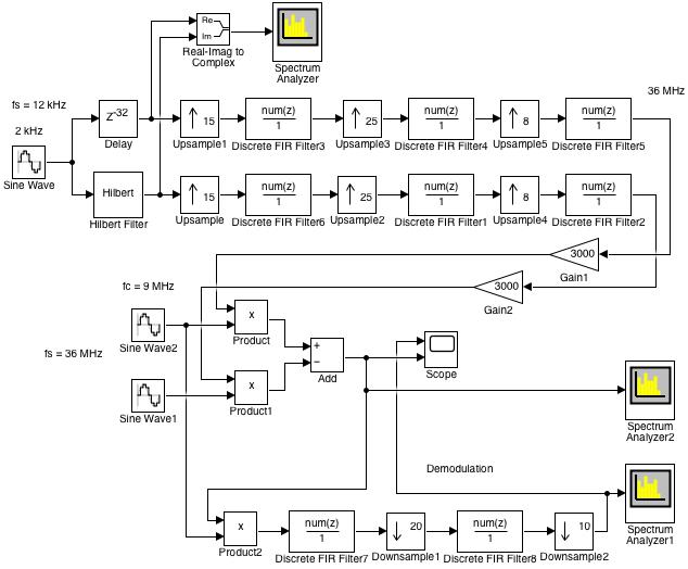
FIR filters are used here for the interpolation. In practice, however, these are CIC filters [2], [4]. The spectrum of the bandpass signal with a carrier with the frequency 9 MHz is shown in Fig. 33, as displayed by the ‘Spectrum Analyzer2’ block.
The simple demodulation of the USB bandpass signal is formed in the lower part of the model. The required carrier is taken over by the carrier of the modulation and therefore it is a synchronous carrier.
The spectrum of the demodulated signal, as it is shown on the Block ‘Spectrum Analyzer1’, is displayed in Fig. 34.
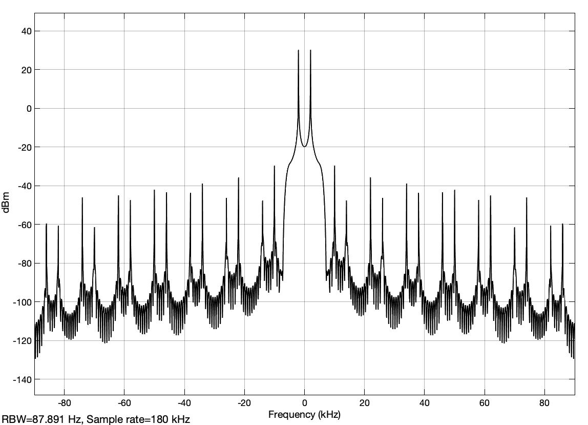
As one can see, the side lobes are well attenuated and the demodulated signal, which is shown with the ‘Scope’ block, has the expected amplitude and, due to the decimation by a factor of 200, the sampling rate is equal to 36 MHz / 200 = 180 kHz >> 12 kHz. This ensures a good resolution of the result.
Remarks
In the simulations, the digital filters are FIR filters, which are determined with the simple function ‘fir1’. This function requires few parameters that are easy to understand. For example with ‘fir1(128, 0.15);’ a FIR low-pass filter of order 128 and relative frequency based on half the sampling frequency of 0.15 is determined. For decimation and interpolation with factor M, the corresponding filter is set with ‘fir1(ord, 1/M);’.
A bandpass filter with pass frequencies f1 = 50 Hz to f2 = 200 Hz with a sampling frequency fs = 1000 Hz and order ord is calculated with the following call: ‘fir1(ord, [f1, f2]*2/fs);’. Other functions such as ‘firgr’ or ‘firpm’ can also be used to optimize the filters with specific parameters.
The analog filters in some of the simulations have to be developed in the ‘Workspace’ before starting the simulation with the function shown in the models.
Once you have familiarized yourself with the simulations, you should try to make the simulations more flexible. The parameters should be declared as variables in the blocks, which are then initialized from a MATLAB script which also calls the simulation. Some variables of the model should be temporarily stored with blocks ‘To Workspace’ in order to represent them with your own ideas with the ‘plot’ function.
The ‘Spectrum Analyzer’ blocks can be parameterized for power, power spectral density or effective values and you can also choose the units so that a linear or a logarithmic representation is implemented.
References
1) Richard Lyons “Understanding the ‘Phasing Method’ of Single Sideband Demodulation”
2) Richard G. Lyons, “Understanding Digital Signal Processing” 3 Edition, Prentice Hall 2010
3) Richard Lyons “Understanding cascaded integrator-comb filters”
4) E. Hogenauer, “An Economical Class of Digital Filters For Decimation and Interpolation,” IEEE Trans. Acoust. Speech and Signal Proc., Vol. ASSP–29, pp. 155–162, April 1981.
5) Fred Harris, “Let’s Assume the System Is Synchronized”
6) Edward W. Kamen, Bonnie S. Heck, “Fundamentals of Signals and Systems, Using MATLAB”, Prentice Hall 1997
- Comments
- Write a Comment Select to add a comment
Amazing artcile . thanks a lot
To post reply to a comment, click on the 'reply' button attached to each comment. To post a new comment (not a reply to a comment) check out the 'Write a Comment' tab at the top of the comments.
Please login (on the right) if you already have an account on this platform.
Otherwise, please use this form to register (free) an join one of the largest online community for Electrical/Embedded/DSP/FPGA/ML engineers:


