


Virtual Analog Example: Phasing
As mentioned in §5.4, the phaser, or phase shifter works by sweeping notches through a signal's short-time spectrum. The notches are classically spaced nonuniformly, while flangers employ uniformly spaced notches (§5.3). In this section, we look at using a chain of allpass filters to implement the phasing effect.
Phasing with First-Order Allpass Filters
The block diagram of a typical inexpensive phase shifter for
guitar players is shown in Fig.8.23.9.20 It
consists of a series chain of first-order allpass
filters,9.21 each having a single time-varying parameter ![]() controlling the pole and zero location over time, plus a feedforward
path through gain
controlling the pole and zero location over time, plus a feedforward
path through gain ![]() which is a fixed depth control. Thus,
the delay line of the flanger is replaced by a string of allpass
filters. (A delay line is of course an allpass filter itself.)
which is a fixed depth control. Thus,
the delay line of the flanger is replaced by a string of allpass
filters. (A delay line is of course an allpass filter itself.)
![\includegraphics[width=4.2in]{eps/allpass1phaser}](http://www.dsprelated.com/josimages_new/pasp/img1891.png)
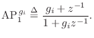
In analog hardware, the first-order allpass transfer function [449, Appendix E, Section 8]9.22is
(In classic phaser circuits such as the Univibe,
Classic Analog Phase Shifters
Setting ![]() in Eq.
in Eq.![]() (8.19) gives the frequency response
of the analog-phaser transfer function to be
(8.19) gives the frequency response
of the analog-phaser transfer function to be
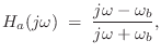
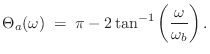
Figure 8.24a shows the phase responses of four first-order analog
allpass filters with ![]() set to
set to
![]() .
Figure 8.24b shows the resulting normalized amplitude response for
the phaser, for
.
Figure 8.24b shows the resulting normalized amplitude response for
the phaser, for ![]() (unity feedfoward gain). The amplitude response
has also been normalized by dividing by 2 so that the maximum gain is
1. Since there is an even number (four) of allpass sections, the gain
at dc is
(unity feedfoward gain). The amplitude response
has also been normalized by dividing by 2 so that the maximum gain is
1. Since there is an even number (four) of allpass sections, the gain
at dc is
![]() . Put another way, the initial
phase of each allpass section at dc is
. Put another way, the initial
phase of each allpass section at dc is ![]() , so that the total
allpass-chain phase at dc is
, so that the total
allpass-chain phase at dc is ![]() . As frequency increases, the
phase of the allpass chain decreases. When it comes down to
. As frequency increases, the
phase of the allpass chain decreases. When it comes down to ![]() ,
the net effect is a sign inversion by the allpass chain, and the
phaser has a notch. There will be another notch when the phase falls
down to
,
the net effect is a sign inversion by the allpass chain, and the
phaser has a notch. There will be another notch when the phase falls
down to ![]() . Thus, four first-order allpass sections give two
notches. For each notch in the desired response we must add two new
first-order allpass sections.
. Thus, four first-order allpass sections give two
notches. For each notch in the desired response we must add two new
first-order allpass sections.
![\includegraphics[width=\twidth]{eps/phaser1a}](http://www.dsprelated.com/josimages_new/pasp/img1910.png) |
From Fig.8.24b, we observe that the first notch is near ![]() Hz. This happens to be the frequency at which the first allpass pole
``breaks,'' i.e.,
Hz. This happens to be the frequency at which the first allpass pole
``breaks,'' i.e.,
![]() . Since the phase of a first-order
allpass section at its break frequency is
. Since the phase of a first-order
allpass section at its break frequency is ![]() , the sum of the
other three sections must be approximately
, the sum of the
other three sections must be approximately
![]() .
Equivalently, since the first section has ``given up''
.
Equivalently, since the first section has ``given up'' ![]() radians
of phase at
radians
of phase at
![]() , the other three allpass sections
combined have given up
, the other three allpass sections
combined have given up ![]() radians as well (with the second
section having given up more than the other two).
radians as well (with the second
section having given up more than the other two).
In practical operation, the break frequencies must change dynamically, usually periodically at some rate.
Classic Virtual Analog Phase Shifters
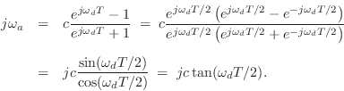
To create a virtual analog phaser, following closely the design
of typical analog phasers, we must translate each first-order allpass
to the digital domain. Working with the transfer function, we must
map from ![]() plane to the
plane to the ![]() plane. There are several ways to
accomplish this goal [362]. However, in this case,
an excellent choice is the bilinear transform (see §7.3.2),
defined by
plane. There are several ways to
accomplish this goal [362]. However, in this case,
an excellent choice is the bilinear transform (see §7.3.2),
defined by
where
Thus, given a particular desired break-frequency
![]() , we can set
, we can set
Recall from Eq.![]() (8.19) that the transfer function of the
first-order analog allpass filter is given by
(8.19) that the transfer function of the
first-order analog allpass filter is given by
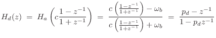
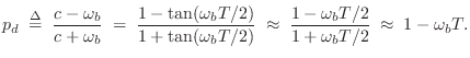
Figure 8.25 shows the digital phaser response curves corresponding
to the analog response curves in Fig.8.24. While the break
frequencies are preserved by construction, the notches have moved
slightly, although this is not visible from the plots. An overlay of
the total phase of the analog and digital allpass chains is shown in
Fig.8.26. We see that the phase responses of the analog and
digital alpass chains diverge visibly only above 9 kHz. The analog
phase response approaches zero in the limit as
![]() ,
while the digital phase response reaches zero at half the sampling
rate,
,
while the digital phase response reaches zero at half the sampling
rate, ![]() kHz in this case. This is a good example of when the
bilinear transform performs very well.
kHz in this case. This is a good example of when the
bilinear transform performs very well.
![\includegraphics[width=\twidth]{eps/phaser1d}](http://www.dsprelated.com/josimages_new/pasp/img1925.png) |
![\includegraphics[width=\twidth]{eps/phaser1ad}](http://www.dsprelated.com/josimages_new/pasp/img1926.png) |
In general, the bilinear transform works well to digitize feedforward analog structures in which the high-frequency warping is acceptable. When frequency warping is excessive, it can be alleviated by the use of oversampling; for example, the slight visible deviation in Fig.8.26 below 10 kHz can be largely eliminated by increasing the sampling rate by 15% or so. See the case of digitizing the Moog VCF for an example in which the presence of feedback in the analog circuit leads to a delay-free loop in the digitized system [479,477].
Phasing with 2nd-Order Allpass Filters
The allpass structure proposed in [429] provides a convenient means for generating nonuniformly spaced notches that are independently controllable to a high degree. An advantage of the allpass approach even in the case of uniformly spaced notches (which we call flanging, as introduced in §5.3) is that no interpolating delay line is needed.
![\includegraphics[width=4.2in]{eps/allpassphaser}](http://www.dsprelated.com/josimages_new/pasp/img1927.png)
The architecture of the phaser based on second-order allpasses is
shown in Fig.8.27. It is identical to that in
Fig.8.23 with each first-order allpass being replaced by
a second-order allpass. I.e., replace
![]() in
Fig.8.23 by
in
Fig.8.23 by
![]() , for
, for ![]() , to get
Fig.8.27. The phaser will have a notch wherever the phase
of the allpass chain is at
, to get
Fig.8.27. The phaser will have a notch wherever the phase
of the allpass chain is at ![]() (180 degrees). It can be shown that
these frequencies occur very close to the resonant frequencies of the
allpass chain [429].
It is therefore convenient to use a single conjugate pole pair in each
allpass section, i.e., use second-order allpass sections of the form
(180 degrees). It can be shown that
these frequencies occur very close to the resonant frequencies of the
allpass chain [429].
It is therefore convenient to use a single conjugate pole pair in each
allpass section, i.e., use second-order allpass sections of the form


and ![]() is the radius of each pole in the complex-conjugate pole pair,
and pole angles are
is the radius of each pole in the complex-conjugate pole pair,
and pole angles are ![]() . The pole angle can be interpreted as
. The pole angle can be interpreted as
![]() where
where ![]() is the resonant frequency and
is the resonant frequency and
![]() is the sampling interval.
is the sampling interval.
Phaser Notch Parameters
To move just one notch, the tuning of the pole-pair in the
corresponding section is all that needs to be changed. Note that
tuning affects only one coefficient in the second-order allpass
structure. (Although the coefficient ![]() appears twice in the
transfer function, it only needs to be used once per sample in a
slightly modified direct-form implementation [449].)
appears twice in the
transfer function, it only needs to be used once per sample in a
slightly modified direct-form implementation [449].)
The depth of the notches can be varied together by changing the gain of the feedforward path.
The bandwidth of individual notches is mostly controlled by the distance of the associated pole-pair from the unit circle. So to widen the notch associated with a particular allpass section, one may increase the ``damping'' of that section.
Finally, since the gain of the allpass string is unity (by definition of allpass filters), the gain of the entire structure is strictly bounded between 0 and 2. This property allows arbitrary notch controls to be applied without fear of the overall gain becoming ill-behaved.
Phaser Notch Distribution
As mentioned above, it is desirable to avoid exact harmonic spacing of the notches, but what is the ideal non-uniform spacing? One possibility is to space the notches according to the critical bands of hearing, since essentially this gives a uniform notch density with respect to ``place'' along the basilar membrane in the ear. There is no need to follow closely the critical-band structure, so that simple exponential spacing may be considered sufficiently perceptually uniform (corresponding to uniform spacing on a log frequency scale). Due to the immediacy of the relation between notch characteristics and the filter coefficients, the notches can easily be placed under musically meaningful control.
Next Section:
Electric Guitars
Previous Section:
Extracting Parametric Resonators from a Nonparametric Impulse Response


