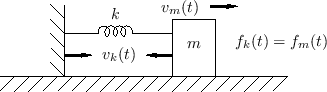
Wave Digital Filters
A Wave Digital Filter (WDF) [136] is a particular kind of digital filter based on physical modeling principles. Unlike most digital filter types, every delay element in a WDF can be interpreted physically as holding the current state of a mass or spring (or capacitor or inductor). WDFs can also be viewed as a particular kind of finite difference scheme having unusually good numerical properties [55]. (See Appendix D for an introduction to finite difference schemes.) WDFs have been applied often in music signal processing [394,338,556,361,348,554,555,56,527,523,484].
Wave digital filters were developed initially by Alfred Fettweis [135] in the late 1960s for digitizing lumped electrical circuits composed of inductors, capacitors, resistors, transformers, gyrators, circulators, and other elements of classical network theory [136]. The WDF approach is based on the traveling-wave formulation of lumped electrical elements introduced by Belevitch [34].
A WDF is constructed by interconnecting simple discrete-time models of individual masses, springs, and dashpots (or inductors, capacitors, and resistors). The rules for interconnecting the elementary models are based on scattering theory (discussed in §C.8). This is a direct result of the fact that all signals explicitly computed may be physically interpreted as traveling wave components of physical variables.
Wave Digital Elements
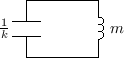
When modeling mechanical systems composed of masses, springs, and dashpots, it is best to begin with an electrical equivalent circuit. Equivalent circuits make clear the network-theoretic structure of the system, clearly indicating, for example, whether interacting elements should be connected in series or parallel. Each element of the equivalent circuit can then be replaced by a first-order wave digital element, and the elements are finally parallel or series connected by means of scattering-junction interfaces known as adaptors.
Wave digital elements may be derived from their describing differential equations (in continuous time) as follows:
- First express
all physical quantities (such as force and velocity) in terms of
traveling-wave components. The traveling wave components are called
wave variables. For example, the force
 on a mass is
decomposed as
on a mass is
decomposed as
 , where
 is regarded as a
traveling wave propagating toward the mass, while
is regarded as a
traveling wave propagating toward the mass, while
 is
seen as the traveling component propagating
away from the mass. A ``traveling wave'' view of
force mediation is actually much closer to physical reality than any
instantaneous model.
is
seen as the traveling component propagating
away from the mass. A ``traveling wave'' view of
force mediation is actually much closer to physical reality than any
instantaneous model.
- Second, digitize the resulting traveling-wave system using the
bilinear transform. The bilinear transform is equivalent in
the time domain to the
trapezoidal rule for numerical integration (see §7.3.2).
- Connect
 elementary units together by means of
-port scattering junctions. There are two basic
types of scattering junction, one for parallel, and one for series
connection. (See §C.8 for the theory of scattering junctions.)
elementary units together by means of
-port scattering junctions. There are two basic
types of scattering junction, one for parallel, and one for series
connection. (See §C.8 for the theory of scattering junctions.)
An important benefit of introducing wave variables prior to bilinear transformation is the elimination of delay-free loops when connecting elementary building blocks. In other words, any number of elementary models can be interconnected, in series or in parallel, and the resulting finite-difference scheme remains explicit (free of delay-free loops).
A Physical Derivation of Wave Digital Elements
This section provides a ``physical'' derivation of Wave Digital Filters (WDF), which contrasts somewhat with the more formal derivation common in the literature. The derivation is presented as a numbered series of steps (some with rather long discussions):
- To each element, such as a capacitor or inductor, attach a
length of waveguide (electrical transmission line) having wave
impedance
 , and make it infinitesimally long. (Take the limit as
its length goes to zero.) A schematic depiction of this is shown in
Fig.F.1a. For consistency, all signals are Laplace transforms of
their respective time-domain signals. The length must approach zero
in order not to introduce propagation delays into the signal path.
, and make it infinitesimally long. (Take the limit as
its length goes to zero.) A schematic depiction of this is shown in
Fig.F.1a. For consistency, all signals are Laplace transforms of
their respective time-domain signals. The length must approach zero
in order not to introduce propagation delays into the signal path.
Figure F.1: a) Physical schematic for the derivation of a wave digital model of driving-point impedance  . The inserted
waveguide impedance is real and positive, but otherwise
arbitrary. b) Expanded view of the interior of the infinitesimal
waveguide section, also representing the termination impedance
as an impedance-step within the waveguide.
. The inserted
waveguide impedance is real and positive, but otherwise
arbitrary. b) Expanded view of the interior of the infinitesimal
waveguide section, also representing the termination impedance
as an impedance-step within the waveguide.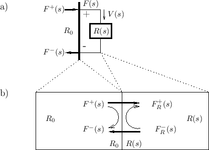
Points to note:
- The infinitesimal waveguide is terminated by the element.
The element reflects waves as if it were a new waveguide section at
impedance , as depicted in Fig.F.1b.
- The interface to the element is recast as traveling-wave
components
 and
and  at impedance .
In terms of these components, the physical force on the element is
obtained by adding them together:
at impedance .
In terms of these components, the physical force on the element is
obtained by adding them together:
 .
.
- The waveguide impedance is arbitrary because it
has been physically introduced. We will need to know it when we
connect this element to other elements. The element's interface to
other elements is now a waveguide (transmission line) at real
impedance .
- The junction is ``parallel'' (cf. §7.2):
- Force (voltage) must be continuous across the junction, since
otherwise there would be a finite force across a zero mass, producing
infinite acceleration.
- The sum of velocities (currents) into the junction must be zero
by conservation of mass (charge).
- Force (voltage) must be continuous across the junction, since
otherwise there would be a finite force across a zero mass, producing
infinite acceleration.
- The infinitesimal waveguide is terminated by the element.
The element reflects waves as if it were a new waveguide section at
impedance
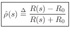
Reflectance of a General Lumped Waveguide Termination
Calculate the reflectance of the terminated waveguide. That is, find the Laplace transform of the return wave divided by the Laplace transform of the input wave going into the waveguide. In general, the reflectance of an impedance step for force waves (voltage waves in the electrical case) is
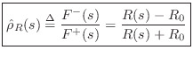
This is easily derived from continuity constraints across the junction. Specifically, referring to Fig.F.1b, let

By the definition of wave impedance in a waveguide, we have
Thus,
![\begin{eqnarray*}
0 &=& V(s) + V_R(s)\\
&=& \left[V^{+}(s)+V^{-}(s)\right] + ...
...s)}\right]
&=& \frac{2}{R_0}F^{+}(s) + \frac{2}{R(s)}F^{+}_R(s)
\end{eqnarray*}](http://www.dsprelated.com/josimages_new/pasp/img4758.png)
Defining
![]() and
and
![]() , we have
, we have
Now that we've solved for the junction force
Finally, the force-wave reflectance of an impedance step from
as claimed.
Reflectances of Elementary Impedances
We now derive the reflectances of the elements used in LTI analog electric circuits, viz., the capacitor, inductor, and resistor.
Capacitor Reflectance
For a capacitor of ![]() Farads, the driving-point impedance is (see
§7.1.3)
Farads, the driving-point impedance is (see
§7.1.3)
Inductor Reflectance
For an inductor of ![]() Henrys, we have
Henrys, we have
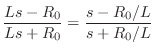
Resistor Reflectance
Finally, for a resistor of ![]() Ohms, we get
Ohms, we get
Note that both the capacitor and inductor reflectances are
stable allpass filters, as they must be. Also, the resistor
reflectance is always less than 1, no matter what waveguide impedance
![]() we choose.
we choose.
Choosing Impedance to Simplify Element Reflectance
Observe that there is a natural choice for each waveguide impedance which will give us a normalized, ``universal reflectance'' for each element:
- For the capacitor, setting
 gives
gives
- For the inductor, setting
 gives
gives
- And for the resistor, we set
 to obtain

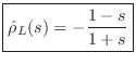
Digitizing Elementary Reflectances by Bilinear Transform
Going to discrete time via the bilinear transform means making the substitution
 |
(F.11) |
where
Solving for ![]() gives us the inverse bilinear transform:
gives us the inverse bilinear transform:
In this case, we see that setting ![]() further simplifies our
universal reflectances in the digital domain:
further simplifies our
universal reflectances in the digital domain:
- For the ``wave digital capacitor'' (or spring), Eq.
 (F.8) becomes
- For the ``wave digital inductor'' (or mass), Eq.(F.9) becomes
- And for the ``wave digital resistor'' (or dashpot), Eq.(F.10) becomes
as before in the continuous-time case.
Note that this choice of ![]() is also the only one that eliminates
delay-free paths in the fundamental elements. This allows them to
be used as building blocks for explicit finite difference
schemes.
is also the only one that eliminates
delay-free paths in the fundamental elements. This allows them to
be used as building blocks for explicit finite difference
schemes.
We may still obtain the above results using the more typical value
![]() (instead of
(instead of ![]() ) in the bilinear transform. From
Eq.
) in the bilinear transform. From
Eq.![]() (F.12), it is clear that changing
(F.12), it is clear that changing ![]() amounts to a linear
frequency scaling of
amounts to a linear
frequency scaling of ![]() . Such a scaling may be compensated
by choosing the waveguide (port) impedances to be
. Such a scaling may be compensated
by choosing the waveguide (port) impedances to be
![]() (instead of
(instead of ![]() ) for the inductor, and
) for the inductor, and
![]() (instead of
(instead of
![]() ) for the capacitor.
) for the capacitor.
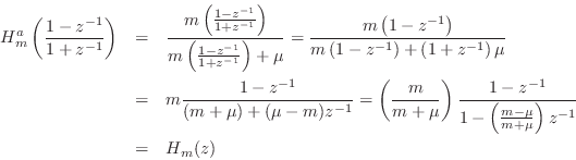
Summary of Wave Digital Elements
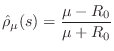
From Eq.![]() (F.1), we have that the general reflectance of impedance
(F.1), we have that the general reflectance of impedance
![]() with respect to the reference impedance
with respect to the reference impedance ![]() in the wave
variable formulation is given by
in the wave
variable formulation is given by
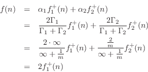
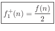
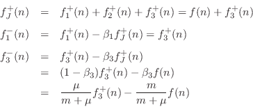
In WDF construction, the free constant in the bilinear transform is taken to be
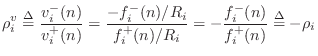
Wave Digital Mass
In the case of a mass ![]() , we have
, we have
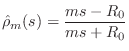
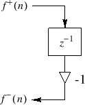 |
Thus, the wave digital mass is simply a unit-sample delay and a negation. The fact that the value of the mass has been canceled out will be addressed below in the subsection on ``adaptors,'' i.e., it only affects interconnection with other elements. For now, just remember that the reference impedance was chosen to be equal to the mass in order to get this simple wave flow diagram. Also note that the WDF mass simulator has no delay-free path from input to output.
Wave Digital Spring
In the case of a spring with stiffness ![]() , we have the impedance
, we have the impedance
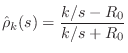
![$\displaystyle \fbox{$\displaystyle \hat{\tilde{\rho}}_k(z) = z^{-1}$} \qquad\makebox[0pt][l]{(Wave Digital Spring)}
$](http://www.dsprelated.com/josimages_new/pasp/img4811.png)
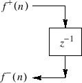
Thus, the WDF of a spring is simply a unit-sample delay, which is just the negative of the WDF mass. If we were to switch to velocity waves instead of force waves, both masses and springs would again correspond to unit-sample delays, but the spring would become inverting and the mass non-inverting.
Wave Digital Dashpot
Starting with a dashpot with coefficient ![]() , we have
, we have
In the context of waveguide theory, a zero reflectance corresponds to a matched impedance, i.e., the terminating transmission-line impedance equals the characteristic impedance of the line.
The difference equation for the wave digital dashpot is simply
![]() . While this may appear overly degenerate at first,
remember that the interface to the element is a port at impedance
. While this may appear overly degenerate at first,
remember that the interface to the element is a port at impedance
![]() . Thus, in this particular case only, the infinitesimal
waveguide interface is the element itself.
. Thus, in this particular case only, the infinitesimal
waveguide interface is the element itself.
Limiting Cases
The force-wave reflectance of an infinite impedance (rigid wall or ``open circuit'') is
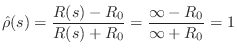
Similarly, the force-wave reflectance of a zero impedance (free termination, frictionless surface, or ``short circuit'') is
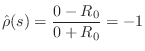
For velocity waves, we obtain the opposite results: rigid terminations are inverting, and free terminations are non-inverting.
Unit Elements
The unit element two-port is simply a bidirectional delay line with half a sample delay in each direction. As a result, it really belongs under the topic of distributed modeling. To avoid delay-free loops, Fettweis noted [135] that every pair of adaptors must be separated by at least one unit element. More recently, this objective is accomplished instead using ``reflection-free ports'' [136] (see also §F.2.2).
Adaptors for Wave Digital Elements
An adaptor is an ![]() -port memoryless interface which
interconnects wave digital elements. Since each element's ``port'' is
a connection to an infinitesimal waveguide section at some real wave
impedance
-port memoryless interface which
interconnects wave digital elements. Since each element's ``port'' is
a connection to an infinitesimal waveguide section at some real wave
impedance ![]() , and since the input/output signals are wave
variables (traveling-waves within the waveguide), the adaptor must
implement signal scattering appropriate for the connection of
such waveguides. In other words, an
, and since the input/output signals are wave
variables (traveling-waves within the waveguide), the adaptor must
implement signal scattering appropriate for the connection of
such waveguides. In other words, an ![]() -port adaptor in a wave
digital filter performs exactly the same computation as an
-port adaptor in a wave
digital filter performs exactly the same computation as an ![]() -port
scattering junction in a digital waveguide network.F.2
-port
scattering junction in a digital waveguide network.F.2
This section first addresses the simpler two-port case, followed by a
derivation of the general ![]() -port adaptor, for both parallel and
series connections of wave digital elements.
-port adaptor, for both parallel and
series connections of wave digital elements.
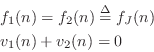
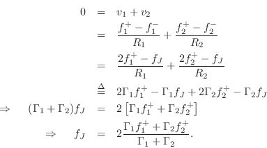
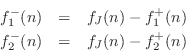
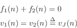
As discussed in §7.2, a physical connection of two or more ports can either be in parallel (forces are equal and the velocities sum to zero) or in series (velocities equal and forces sum to zero). Combinations of parallel and series connections are also of course possible.
Two-Port Parallel Adaptor for Force Waves
Figure F.5a illustrates a generic parallel two-port connection in terms of forces and velocities.
![\includegraphics[width=\twidth]{eps/lAdaptorParallel}](http://www.dsprelated.com/josimages_new/pasp/img4823.png) |
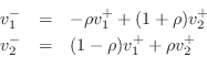
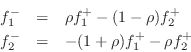
As discussed in §7.2, a parallel connection is characterized by a common force and velocities which sum to zero:
Following the same derivation leading to Eq.![]() (F.2), and defining
(F.2), and defining
![]() for notational convenience, we obtain
for notational convenience, we obtain
The outgoing wave variables are given by
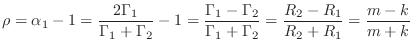
Defining the reflection coefficient as

as diagrammed in Fig.F.5b. This can be called the Kelly-Lochbaum implementation of the two-port force-wave adaptor.
Now that we have a proper scattering interface between two reference
impedances, we may connect two wave digital elements together, setting
![]() to the port impedance of element 1, and
to the port impedance of element 1, and ![]() to the port
impedance of element 2. An example is shown in Fig.F.35.
to the port
impedance of element 2. An example is shown in Fig.F.35.
The Kelly-Lochbaum adaptor in Fig.F.5b evidently requires four multiplies and two additions. Note that we can factor out the reflection coefficient in each equation to obtain
which requires only one multiplication and three additions. This can be called the one-multiply form. The one-multiply form is most efficient in custom VLSI. The Kelly-Lochbaum form, on the other hand, may be more efficient in software, and slightly faster (by one addition) in parallel hardware.
Compatible Port Connections
Note carefully that to connect a wave digital element to port
![]() of the adaptor, we route the signal
of the adaptor, we route the signal
![]() coming out of the
element to become
coming out of the
element to become
![]() on the adaptor port, and the signal
on the adaptor port, and the signal
![]() coming out of port
coming out of port ![]() of the adaptor goes into the element
as
of the adaptor goes into the element
as
![]() . Such a connection is said to be a
compatible port connection. In other words, the connections
must be made such that the arrows go in the same direction in the wave
flow diagram.
. Such a connection is said to be a
compatible port connection. In other words, the connections
must be made such that the arrows go in the same direction in the wave
flow diagram.
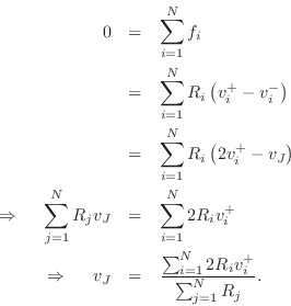
General Parallel Adaptor for Force Waves
In the more general case of ![]() wave digital element ports being
connected in parallel, we have the physical constraints
wave digital element ports being
connected in parallel, we have the physical constraints
| (F.14) | |||
| (F.15) |
The derivation for the two-port case extends to the


The outgoing wave variables are given by
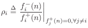
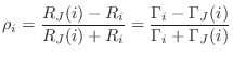
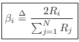
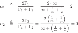
Alpha Parameters
It is customary in the wave digital filter literature to define the alpha parameters as
where

We see that

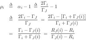
Reflection Coefficient, Parallel Case
The reflection coefficient seen at port ![]() is defined as
is defined as
In other words, the reflection coefficient specifies what portion of the incoming wave
where
Equating like terms with Eq.![]() (F.21), we obtain
(F.21), we obtain
Thus, the
Physical Derivation of Reflection Coefficient
Physically, the reflection coefficient seen at port ![]() is due to an
impedance step from
is due to an
impedance step from ![]() , that of the port interface, to a new
impedance consisting of the parallel combination of all other
port impedances meeting at the junction. Let
, that of the port interface, to a new
impedance consisting of the parallel combination of all other
port impedances meeting at the junction. Let
denote this parallel combination, in admittance form. Then we must have
Let's check this ``physical'' derivation against the formal definition
Eq.![]() (F.20) leading to
(F.20) leading to
![]() in Eq.
in Eq.![]() (F.22).
Toward this goal, let
(F.22).
Toward this goal, let

and the result is verified.
Reflection Free Port
It is useful in practice, such as when connecting two adaptors
together, to make one port reflection free. A
reflection-free port is defined to have a zero reflection coefficient. For port
![]() of a parallel adaptor to be reflection free, we must have, from
Eq.
of a parallel adaptor to be reflection free, we must have, from
Eq.![]() (F.25),
(F.25),
Connecting two adaptors at a reflection-free port prevents the formation of a delay-free loop which would otherwise occur [136]. As a result, multi-port junctions can be joined without having to insert unit elements (see §F.1.7) to avoid creating delay-free loops. Only one of the two ports participating in the connection needs to be reflection free.
We can always make a reflection-free port at the connection of two adaptors because the ports used for this connection (one on each adaptor) were created only for purposes of this connection. They can be set to any impedance, and only one of them needs to be reflection free.
To interconnect three adaptors, labeled ![]() ,
, ![]() , and
, and ![]() , we may
proceed as follows: Let
, we may
proceed as follows: Let ![]() be augmented with two unconstrained
ports, having impedances
be augmented with two unconstrained
ports, having impedances ![]() and
and ![]() . Add a reflection-free
port to
. Add a reflection-free
port to ![]() , and suppose its impedance has to be
, and suppose its impedance has to be ![]() . Add a
reflection-free port to
. Add a
reflection-free port to ![]() , and suppose its impedance has to be
, and suppose its impedance has to be
![]() . Now set
. Now set ![]() and connect
and connect ![]() to
to ![]() via the
corresponding ports. Similarly, set
via the
corresponding ports. Similarly, set ![]() and connect
and connect ![]() to
to ![]() accordingly. This adaptor-connection protocol clearly extends to any
number of adaptors.
accordingly. This adaptor-connection protocol clearly extends to any
number of adaptors.
Two-Port Series Adaptor for Force Waves
Figure F.6a illustrates a generic two-port description of the series adaptor.
![\includegraphics[width=\twidth]{eps/lAdaptorSeries}](http://www.dsprelated.com/josimages_new/pasp/img4871.png) |
As discussed in §7.2, a series connection is characterized by a common velocity and forces which sum to zero at the junction:
The derivation can proceed exactly as for the parallel junction in
§F.2.1, but with force and velocity interchanged, i.e.,
![]() , and with impedance and admittance interchanged,
i.e.,
, and with impedance and admittance interchanged,
i.e.,
![]() . In this way, we may take the
dual of Eq.
. In this way, we may take the
dual of Eq.![]() (F.14) to get
(F.14) to get
diagrammed in Fig.F.7. Converting back to force wave
variables via
![]() and
and
![]() , and noting
that
, and noting
that
![]() , we obtain, finally,
, we obtain, finally,
as diagrammed in Fig.F.6b. The one-multiply form is now
![\includegraphics[scale=0.9]{eps/lscat_vel_series_renum}](http://www.dsprelated.com/josimages_new/pasp/img4881.png)
General Series Adaptor for Force Waves
In the more general case of ![]() ports being connected in
series, we have the physical constraints
ports being connected in
series, we have the physical constraints

The derivation is the dual of that in the parallel case (cf.
Eq.![]() (F.16)), i.e., force and velocity are interchanged, and impedance
and admittance are interchanged:
(F.16)), i.e., force and velocity are interchanged, and impedance
and admittance are interchanged:
The outgoing wave variables are given by
Beta Parameters
It is customary in the wave digital filter literature to define the beta parameters as
where

However, we normally employ a mixture of parallel and series adaptors,
while keeping a force-wave simulation. Since
![]() , we obtain, after a small amount of algebra, the following
recipe for the series force-wave adaptor:
, we obtain, after a small amount of algebra, the following
recipe for the series force-wave adaptor:

We see that we have

Reflection Coefficient, Series Case
The velocity reflection coefficient seen at port
![]() is defined as
is defined as
Representing the outgoing velocity wave
where
Equating like terms with Eq.![]() (F.32) gives
(F.32) gives
Thus, the
Physical Derivation of Series Reflection Coefficient
Physically, the force-wave reflection coefficient seen at port
![]() of a series adaptor is due to an impedance step from
of a series adaptor is due to an impedance step from ![]() , that
of the port interface, to a new impedance consisting of the series
combination of all other port impedances meeting at the
junction. Let
, that
of the port interface, to a new impedance consisting of the series
combination of all other port impedances meeting at the
junction. Let
denote this series combination. Then we must have, as in Eq.
 |
(F.36) |
Let's check this ``physical'' derivation against the formal definition
Eq.![]() (F.31) leading to
(F.31) leading to
![]() in Eq.
in Eq.![]() (F.33).
Define the total junction impedance as
(F.33).
Define the total junction impedance as

Since
Series Reflection Free Port
For port ![]() to be reflection free in a series adaptor, we require
to be reflection free in a series adaptor, we require
That is, the port's impedance must equal the series combination of the other port impedances at the junction. This result can be compared with that for the parallel junction in §F.2.2.
The series adaptor has now been derived in a way which emphasizes its duality with respect to the parallel adaptor.
Wave Digital Modeling Examples
This section presents a series of examples, working up from very simple to more complicated situations.
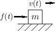
``Piano hammer in flight''
Suppose we wish to model a situation in which a mass of size ![]() kilograms is traveling with a constant velocity. This is an
appropriate model for a piano hammer after its key has been pressed
and before the hammer has reached the string.
kilograms is traveling with a constant velocity. This is an
appropriate model for a piano hammer after its key has been pressed
and before the hammer has reached the string.
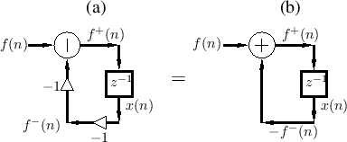
Figure F.2 shows the ``wave digital mass'' derived previously.
The derivation consisted of inserting an infinitesimal
waveguideF.3 having (real) impedance
![]() , solving for the force-wave reflectance of the mass as seen from
the waveguide, and then mapping it to the discrete time domain using
the bilinear transform.
, solving for the force-wave reflectance of the mass as seen from
the waveguide, and then mapping it to the discrete time domain using
the bilinear transform.
We now need to attach the other end of the transmission line to a ``force source'' which applies a force of zero newtons to the mass. In other words, we need to terminate the line in a way that corresponds to zero force.
Let the force-wave components entering and leaving the mass
be denoted ![]() and
and ![]() , respectively (i.e., we are dropping
the subscript `d' in Fig.F.2).
The physical force associated with the mass is
, respectively (i.e., we are dropping
the subscript `d' in Fig.F.2).
The physical force associated with the mass is

Figure F.8a (left portion) illustrates what we derived
by physical reasoning, and as such, it is most appropriate as a
physical model of the constant-velocity mass. However, for actual
implementation, Fig.F.8b would be more typical in
practice. This is because we can always negate the state variable
![]() if needed to convert it from
if needed to convert it from
![]() to
to
![]() . It is
very common to see final simplifications like this to maximize
efficiency.
. It is
very common to see final simplifications like this to maximize
efficiency.
Note that Fig.F.8b can be interpreted physically as a wave
digital spring displaced by a constant force
![]() .
.
Extracting Physical Quantities
Since we are using a force-wave simulation, the state variable ![]() (delay element output) is in units of physical force (newtons).
Specifically,
(delay element output) is in units of physical force (newtons).
Specifically,
![]() . (The physical force is, of
course, 0, while its traveling-wave components are not 0 unless the
mass is at rest.) Using the fundamental relations relating traveling
force and velocity waves
. (The physical force is, of
course, 0, while its traveling-wave components are not 0 unless the
mass is at rest.) Using the fundamental relations relating traveling
force and velocity waves
where ![]() here, it is easy to convert the state variable
here, it is easy to convert the state variable ![]() to
other physical units, as we now demonstrate.
to
other physical units, as we now demonstrate.
The velocity of the mass, for example, is given by

The kinetic energy of the mass is given by
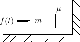
Force Driving a Mass
Suppose now that we wish to drive the mass along a frictionless
surface using a variable force ![]() . This is similar to the
previous example, except that we now want the traveling-wave
components of the force on the mass to sum to
. This is similar to the
previous example, except that we now want the traveling-wave
components of the force on the mass to sum to ![]() instead of 0:
instead of 0:
The simplified form in Fig.F.9b can be interpreted as a wave
digital spring with applied force ![]() delivered from an infinite
source impedance. That is, when the applied force goes to zero, the
termination remains rigid at the current displacement.
delivered from an infinite
source impedance. That is, when the applied force goes to zero, the
termination remains rigid at the current displacement.
A More Formal Derivation of the Wave Digital Force-Driven Mass
Above we derived how to handle the external force by direct physical reasoning. In this section, we'll derive it using a more general step-by-step procedure which can be applied systematically to more complicated situations.
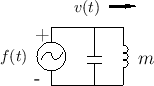
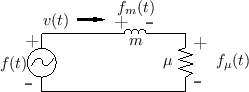
Figure F.10 gives the physical picture of a free mass driven by
an external force in one dimension. Figure F.11 shows the
electrical equivalent circuit for this scenario in which the external
force is represented by a voltage source emitting ![]() volts,
and the mass is modeled by an inductor having the value
volts,
and the mass is modeled by an inductor having the value ![]() Henrys.
Henrys.
 |
The next step is to convert the voltages and currents in the
electrical equivalent circuit to wave variables.
Figure F.12 gives an intermediate equivalent circuit in which
an infinitesimal transmission line section with real impedance ![]() has been inserted to facilitate the computation of the wave-variable
reflectance, as we did in §F.1.1 to derive Eq.
has been inserted to facilitate the computation of the wave-variable
reflectance, as we did in §F.1.1 to derive Eq.![]() (F.1).
(F.1).
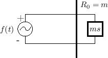 |
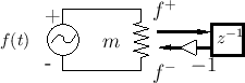
Figure F.13 depicts a next intermediate equivalent circuit in
which the mass has been replaced by its reflectance (using ``![]() ''
to denote the continuous-time reflectance
''
to denote the continuous-time reflectance
![]() , as derived in
§F.1.1). The infinitesimal transmission-line section is now represented
by a ``resistor'' since, when the voltage source is initially
``switched on'', it only ``sees'' a real resistance having the value
, as derived in
§F.1.1). The infinitesimal transmission-line section is now represented
by a ``resistor'' since, when the voltage source is initially
``switched on'', it only ``sees'' a real resistance having the value
![]() Ohms (the waveguide interface). After a short period of time
determined by the reflectance of the mass,F.4 ``return waves'' from the mass result in an ultimately
reactive impedance. This of course must be the case because the
mass does not dissipate energy. Therefore, the ``resistor'' of
Ohms (the waveguide interface). After a short period of time
determined by the reflectance of the mass,F.4 ``return waves'' from the mass result in an ultimately
reactive impedance. This of course must be the case because the
mass does not dissipate energy. Therefore, the ``resistor'' of ![]() Ohms is not a resistor in the usual sense since it does not convert
potential energy (the voltage drop across it) into heat. Instead, it
converts potential energy into propagating waves with 100%
efficiency. Since all of this wave energy is ultimately reflected by
the terminating element (mass, spring, or any combination of masses
and springs), the net effect is a purely reactive impedance, as we
know it must be.
Ohms is not a resistor in the usual sense since it does not convert
potential energy (the voltage drop across it) into heat. Instead, it
converts potential energy into propagating waves with 100%
efficiency. Since all of this wave energy is ultimately reflected by
the terminating element (mass, spring, or any combination of masses
and springs), the net effect is a purely reactive impedance, as we
know it must be.
 |
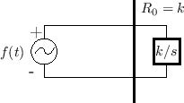
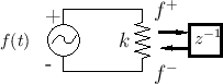
To complete the wave digital model, we need to connect our wave
digital mass to an ideal force source which asserts the value ![]() each sample time. Since an ideal force source has a zero internal
impedance, we desire a parallel two-port junction which connects the
impedances
each sample time. Since an ideal force source has a zero internal
impedance, we desire a parallel two-port junction which connects the
impedances ![]() (
(
![]() ) and
) and ![]() (
(
![]() ), as
shown in Fig.F.14. From
Eq.
), as
shown in Fig.F.14. From
Eq.![]() (F.18) we have that the common junction force is equal to
(F.18) we have that the common junction force is equal to
from which we conclude that

Since
![]() and
and
![]() for this model, the reflection
coefficient seen on port 1 is
for this model, the reflection
coefficient seen on port 1 is
![]() . The
transmission coefficient from port 1 is
. The
transmission coefficient from port 1 is ![]() . In the opposite
direction, the reflection coefficient on port 2 is
. In the opposite
direction, the reflection coefficient on port 2 is ![]() , and
the transmission coefficient from port 2 is
, and
the transmission coefficient from port 2 is
![]() . The final
result, drawn in Kelly-Lochbaum form (see §F.2.1), is
diagrammed in Fig.F.15, as well as the result of some
elementary simplifications. The final model is the same as in
Fig.F.9, as it should be.
. The final
result, drawn in Kelly-Lochbaum form (see §F.2.1), is
diagrammed in Fig.F.15, as well as the result of some
elementary simplifications. The final model is the same as in
Fig.F.9, as it should be.
Force Driving a Spring against a Wall
For this example, we have an external force ![]() driving a spring
driving a spring
![]() which is terminated on the other end at a rigid wall.
Figure F.16 shows the physical diagram
and the electrical equivalent circuit is given in
Fig.F.17.
which is terminated on the other end at a rigid wall.
Figure F.16 shows the physical diagram
and the electrical equivalent circuit is given in
Fig.F.17.
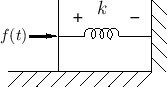
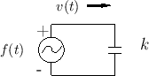
Figure F.18 depicts the insertion of an infinitesimal transmission line, and Fig.F.19 shows the result of converting the spring impedance to wave variable form.
 |
The two-port adaptor needed for this problem is the same as that for the force-driven mass, and the final result is shown in Fig.F.20.
Note that the spring model is being driven by a force from a zero source impedance, in contrast with the infinite source impedance interpretation of Fig.F.8b as a compressed spring. In this case, if the driving force goes to zero, the spring force goes immediately to zero (``free termination'') rather than remaining fixed.
Spring and Free Mass
For this example, we have an external force ![]() driving a spring
driving a spring
![]() which in turn drives a free mass
which in turn drives a free mass ![]() . Since the force on the
spring and the mass are always the same, they are formally
``parallel'' impedances.
. Since the force on the
spring and the mass are always the same, they are formally
``parallel'' impedances.
This problem is easier than it may first appear since an ideal ``force source'' (i.e., one with a zero source impedance) driving impedances in parallel can be analyzed separately for each parallel branch. That is, the system is equivalent to one in which the mass and spring are not connected at all, and each has its own copy of the force source. With this insight in mind, one can immediately write down the final wave-digital model shown in Fig.F.25. However, we will go ahead and analyze this case more formally since it has some interesting features.
Figure F.21 shows the physical diagram of the spring-mass system driven by an external force. The electrical equivalent circuit appears in Fig.F.22, and the first stage of a wave-variable conversion is shown in Fig.F.23.
 |
 |
For this example we need a three-port parallel adaptor, as shown in
Fig.F.24 (along with its attached mass and spring).
The port impedances are 0, ![]() , and
, and ![]() , yielding alpha parameters
, yielding alpha parameters
![]() and
and
![]() . The final result, after the
same sorts of elementary simplifications as in the previous example,
is shown in Fig.F.25. As predicted, a force source driving
elements in parallel is equivalent to a set of independent
force-driven elements.
. The final result, after the
same sorts of elementary simplifications as in the previous example,
is shown in Fig.F.25. As predicted, a force source driving
elements in parallel is equivalent to a set of independent
force-driven elements.
 |
From this and the preceding example, we can see a general pattern:
Whenever there is an ideal force source driving a parallel
junction, then
![]() and all other port admittances are
finite. In this case, we always obtain
and all other port admittances are
finite. In this case, we always obtain
![]() and
and
![]() ,
,
![]() .
.
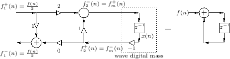
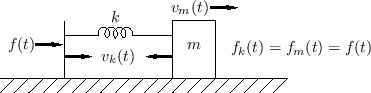
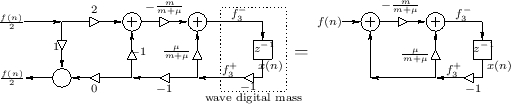
Mass and Dashpot in Series
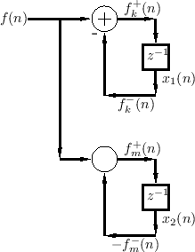
This is our first example illustrating a series connection of wave digital elements. Figure F.26 gives the physical scenario of a simple mass-dashpot system, and Fig.F.27 shows the equivalent circuit. Replacing element voltages and currents in the equivalent circuit by wave variables in an infinitesimal waveguides produces Fig.F.28.
 |
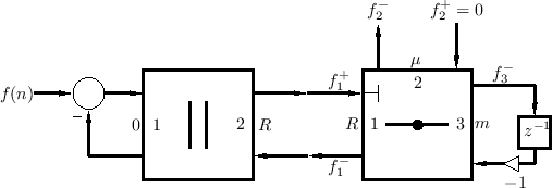 |
The system can be described as an ideal force source ![]() connected
in parallel with the series connection of mass
connected
in parallel with the series connection of mass ![]() and
dashpot
and
dashpot ![]() .
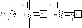
Figure F.29 illustrates the resulting wave digital filter.
Note that the ports are now numbered for reference. Two more symbols
are introduced in this figure: (1) the horizontal line with a dot in
the middle indicating a series adaptor, and (2) the indication of a
reflection-free port on input 1 of the series adaptor (signal
.
Figure F.29 illustrates the resulting wave digital filter.
Note that the ports are now numbered for reference. Two more symbols
are introduced in this figure: (1) the horizontal line with a dot in
the middle indicating a series adaptor, and (2) the indication of a
reflection-free port on input 1 of the series adaptor (signal
![]() ). Recall that a reflection-free port is always necessary
when connecting two adaptors together, to avoid creating a delay-free
loop.
). Recall that a reflection-free port is always necessary
when connecting two adaptors together, to avoid creating a delay-free
loop.
Let's first calculate the impedance ![]() necessary to make input 1 of
the series adaptor reflection free. From Eq.
necessary to make input 1 of
the series adaptor reflection free. From Eq.![]() (F.37), we require
(F.37), we require
The parallel adaptor, viewed alone, is equivalent to a force source
driving impedance ![]() . It is therefore realizable as in
Fig.F.20 with the wave digital spring replaced by the
mass-dashpot assembly in
Fig.F.29. However, we can also carry out a quick analysis
to verify this: The alpha parameters are
. It is therefore realizable as in
Fig.F.20 with the wave digital spring replaced by the
mass-dashpot assembly in
Fig.F.29. However, we can also carry out a quick analysis
to verify this: The alpha parameters are
Therefore, the reflection coefficient seen at port 1 of the parallel
adaptor is
![]() , and the Kelly-Lochbaum scattering
junction depicted in Fig.F.20 is verified.
, and the Kelly-Lochbaum scattering
junction depicted in Fig.F.20 is verified.
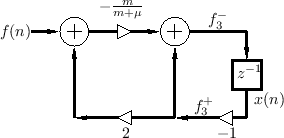
Let's now calculate the internals of the series adaptor in
Fig.F.29. From Eq.![]() (F.26), the beta parameters are
(F.26), the beta parameters are
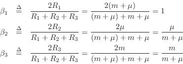
Following Eq.![]() (F.30), the series adaptor computes
(F.30), the series adaptor computes
We do not need to explicitly compute
![]() because it goes into a
purely resistive impedance
because it goes into a
purely resistive impedance ![]() and produces no return wave. For the
same reason,
and produces no return wave. For the
same reason,
![]() .
Figure F.30 shows a wave flow diagram of the computations derived,
together with the result of elementary simplifications.
.
Figure F.30 shows a wave flow diagram of the computations derived,
together with the result of elementary simplifications.
 |
Because the difference of the two coefficients in Fig.F.30 is 1, we can easily derive the one-multiply form in Fig.F.31.
Checking the WDF against the Analog Equivalent Circuit
Let's check our result by comparing the transfer function from the input force to the force on the mass in both the discrete- and continuous-time cases.
For the discrete-time case, we have

We now need
![]() .
To simplify notation, define the two coefficients as
.
To simplify notation, define the two coefficients as

From Figure F.30, we can write
![\begin{eqnarray*}
F^{-}_3(z) &=& -a\left[F(z)-z^{-1}F^{-}_3(z)\right] + b\left[-...
...\,\,\quad
F^{-}_3(z) &=& -a\frac{F(z)}{1-(a-b)z^{-1}F^{-}_3(z)}
\end{eqnarray*}](http://www.dsprelated.com/josimages_new/pasp/img4987.png)
Thus, the desired transfer function is
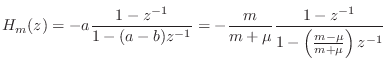
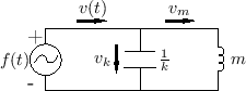
We now wish to compare this result to the bilinear transform of the corresponding analog transfer function. From Figure F.27, we can recognize the mass and dashpot as voltage divider:
Thus, we have verified that the force transfer-function from the driving force to the mass is identical in the discrete- and continuous-time models, except for the bilinear transform frequency warping in the discrete-time case.
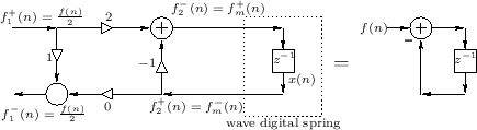
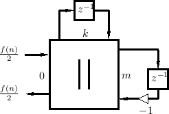
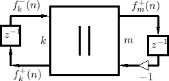
Wave Digital Mass-Spring Oscillator
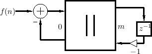
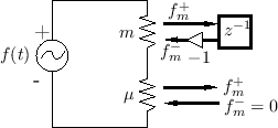
Let's look again at the mass-spring oscillator of §F.3.4, but this time without the driving force (which effectively decouples the mass and spring into separate first-order systems). The physical diagram and equivalent circuit are shown in Fig.F.32 and Fig.F.33, respectively.
Note that the mass and spring can be regarded as being in parallel or
in series. Under the parallel interpretation, we have the WDF shown
in Fig.F.34 and Fig.F.35.F.5
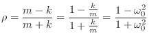
The reflection coefficient ![]() can be computed, as usual, from
the first alpha parameter:
can be computed, as usual, from
the first alpha parameter:
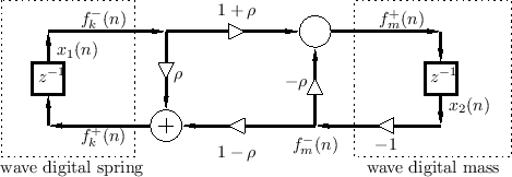
Oscillation Frequency
From Fig.F.33, we can see that the impedance of the parallel combination of the mass and spring is given by

(using the product-over-sum rule for combining impedances in parallel). The poles of this impedance are given by the roots of the denominator polynomial in

The resonance frequency of the mass-spring oscillator is therefore

Since the poles
We can now write reflection coefficient ![]() (see Fig.F.35) as
(see Fig.F.35) as
DC Analysis of the WD Mass-Spring Oscillator
Considering the dc case first (![]() ), we see from Fig.F.35
that the state variable
), we see from Fig.F.35
that the state variable ![]() will circulate unchanged in the
isolated loop on the left. Let's call this value
will circulate unchanged in the
isolated loop on the left. Let's call this value
![]() . Then the physical force on the spring is always equal to
. Then the physical force on the spring is always equal to
The loop on the right in Fig.F.35 receives
At first, this result might appear to contradict conservation of energy, since the state amplitude seems to be growing without bound. However, the physical force is fortunately better behaved:
Since the spring and mass are connected in parallel, it must be the true that they are subjected to the same physical force at all times. Comparing Equations (F.41-F.43) verifies this to be the case.
WD Mass-Spring Oscillator at Half the Sampling Rate
Under the bilinear transform, the ![]() maps to
maps to ![]() (half the
sampling rate). It is therefore no surprise that given
(half the
sampling rate). It is therefore no surprise that given
![]() (
(![]() ), inspection of Fig.F.35 reveals
that any alternating sequence (sinusoid sampled at half the sampling
rate) will circulate unchanged in the loop on the right, which is now
isolated. Let
), inspection of Fig.F.35 reveals
that any alternating sequence (sinusoid sampled at half the sampling
rate) will circulate unchanged in the loop on the right, which is now
isolated. Let
![]() denote this alternating sequence.
The loop on the left receives
denote this alternating sequence.
The loop on the left receives
![]() and adds
and adds
![]() to
it, i.e.,
to
it, i.e.,
![]() .
If we start out with
.
If we start out with ![]() and
and
![]() , we obtain
, we obtain
![]() , or
, or
which agrees with the spring, as it must.
Linearly Growing State Variables in WD Mass-Spring Oscillator
It may seem disturbing that such a simple, passive, physically
rigorous simulation of a mass-spring oscillator should have to make
use of state variables which grow without bound for the limiting cases
of simple harmonic motion at frequencies zero and half the sampling
rate. This is obviously a valid concern in practice as well.
However, it is easy to show that this only happens at dc and ![]() ,
and that there is a true degeneracy at these frequencies, even in the
physics. For all frequencies in the audio range (e.g., for typical
sampling rates), such state variable growth cannot occur. Let's take
closer look at this phenomenon, first from a signal processing point
of view, and second from a physical point of view.
,
and that there is a true degeneracy at these frequencies, even in the
physics. For all frequencies in the audio range (e.g., for typical
sampling rates), such state variable growth cannot occur. Let's take
closer look at this phenomenon, first from a signal processing point
of view, and second from a physical point of view.
A Signal Processing Perspective on Repeated Mass-Spring Poles
Going back to the poles of the mass-spring system in Eq.![]() (F.39),
we see that, as the imaginary part of the two poles,
(F.39),
we see that, as the imaginary part of the two poles,
![]() , approach zero, they come together at
, approach zero, they come together at ![]() to create a
repeated pole. The same thing happens at
to create a
repeated pole. The same thing happens at
![]() since
both poles go to ``the point at infinity''.
since
both poles go to ``the point at infinity''.
It is a well known fact from linear systems theory that two poles at
the same point
![]() in the
in the ![]() plane can correspond to an
impulse-response component of the form
plane can correspond to an
impulse-response component of the form
![]() , in addition
to the component
, in addition
to the component
![]() produced by a single pole at
produced by a single pole at
![]() . In the discrete-time case, a double pole at
. In the discrete-time case, a double pole at ![]() can
give rise to an impulse-response component of the form
can
give rise to an impulse-response component of the form ![]() .
This is the fundamental source of the linearly growing internal states
of the wave digital sine oscillator at dc and
.
This is the fundamental source of the linearly growing internal states
of the wave digital sine oscillator at dc and ![]() . It is
interesting to note, however, that such modes are always
unobservable at any physical output such as the mass
force or spring force that is not actually linearly growing.
. It is
interesting to note, however, that such modes are always
unobservable at any physical output such as the mass
force or spring force that is not actually linearly growing.
Physical Perspective on Repeated Poles in the Mass-Spring System
In the physical system, dc and infinite frequency are in fact strange
cases. In the case of dc, for example, a nonzero constant force
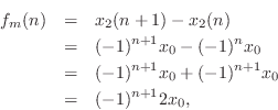
implies that the mass ![]() is under constant acceleration. It is
therefore the case that its velocity is linearly growing. Our
simulation predicts this, since, using
Eq.
is under constant acceleration. It is
therefore the case that its velocity is linearly growing. Our
simulation predicts this, since, using
Eq.![]() (F.43) and Eq.
(F.43) and Eq.![]() (F.42),
(F.42),
![\begin{eqnarray*}
v_m(n) &=& \frac{f^{{+}}_m(n)}{m} - \frac{f^{{-}}_m(n)}{m}
=...
...m} \left[2(n+1) + 2n\right]x_0
= \frac{1}{m} (4 n x_0 + 2 x_0).
\end{eqnarray*}](http://www.dsprelated.com/josimages_new/pasp/img5032.png)
The dc term ![]() is therefore accompanied by a linearly growing
term
is therefore accompanied by a linearly growing
term ![]() in the physical mass velocity. It is therefore
unavoidable that we have some means of producing an unbounded,
linearly growing output variable.
in the physical mass velocity. It is therefore
unavoidable that we have some means of producing an unbounded,
linearly growing output variable.
Mass-Spring Boundedness in Reality
To approach the limit of
![]() , we must either
take the spring constant
, we must either
take the spring constant ![]() to zero, or the mass
to zero, or the mass ![]() to infinity, or
both.
to infinity, or
both.
In the case of ![]() , the constant force must approach zero, and we
are left with at most a constant mass velocity in the limit (not a
linearly growing one, since there can be no dc force at the limit).
When the spring force reaches zero,
, the constant force must approach zero, and we
are left with at most a constant mass velocity in the limit (not a
linearly growing one, since there can be no dc force at the limit).
When the spring force reaches zero, ![]() , so that only zeros
will feed into the loop on the right in Fig.F.35, thus avoiding
a linearly growing velocity, as demanded by the physics. (A constant
velocity is free to circulate in the loop on the right, but the loop
on the left must be zeroed out in the limit.)
, so that only zeros
will feed into the loop on the right in Fig.F.35, thus avoiding
a linearly growing velocity, as demanded by the physics. (A constant
velocity is free to circulate in the loop on the right, but the loop
on the left must be zeroed out in the limit.)
In the case of
![]() , the mass becomes unaffected by the spring
force, so its final velocity must be zero. Otherwise, the attached
spring would keep compressing or stretching forever, and this would
take infinite energy. (Another way to arrive at this conclusion is to
note that the final kinetic energy of the mass would be
, the mass becomes unaffected by the spring
force, so its final velocity must be zero. Otherwise, the attached
spring would keep compressing or stretching forever, and this would
take infinite energy. (Another way to arrive at this conclusion is to
note that the final kinetic energy of the mass would be
![]() .) Since the total energy in an undriven mass-spring
oscillator is always constant, the infinite-mass limit must be
accompanied by a zero-velocity limit.F.6 This means the mass's
state variable
.) Since the total energy in an undriven mass-spring
oscillator is always constant, the infinite-mass limit must be
accompanied by a zero-velocity limit.F.6 This means the mass's
state variable ![]() in Fig.F.35 must be forced to zero in
the limit so that there will be no linearly growing solution at dc.
in Fig.F.35 must be forced to zero in
the limit so that there will be no linearly growing solution at dc.
In summary, when two or more system poles approach each other to form
a repeated pole, care must be taken to ensure that the limit is
approached in a physically meaningful way. In the case of the
mass-spring oscillator, for example, any change in the spring constant
![]() or mass
or mass ![]() must be accompanied by the physically appropriate
change in the state variables
must be accompanied by the physically appropriate
change in the state variables ![]() and/or
and/or ![]() . It is
obviously incorrect, for example, to suddenly set
. It is
obviously incorrect, for example, to suddenly set ![]() in the
simulation without simultaneously clearing the spring's state variable
in the
simulation without simultaneously clearing the spring's state variable
![]() , since the force across an infinitely compliant spring can
only be zero.
, since the force across an infinitely compliant spring can
only be zero.
Similar remarks apply to repeated poles corresponding to
![]() . In this case, the mass and spring basically change
places.
. In this case, the mass and spring basically change
places.
Energy-Preserving Parameter Changes (Mass-Spring Oscillator)
If the change in ![]() or
or ![]() is deemed to be ``internal'', that is,
involving no external interactions, the appropriate accompanying
change in the internal state variables is that which conserves
energy. For the mass and its velocity, for example, we must have
is deemed to be ``internal'', that is,
involving no external interactions, the appropriate accompanying
change in the internal state variables is that which conserves
energy. For the mass and its velocity, for example, we must have
If the spring constant ![]() is to change from
is to change from ![]() to
to ![]() , the
instantaneous spring displacement
, the
instantaneous spring displacement ![]() must satisfy
must satisfy
Exercises in Wave Digital Modeling
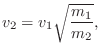
- Comparing digital and analog frequency formulas.
This first exercise verifies that the elementary ``tank circuit''
always resonates at exactly the frequency it should, according to the
bilinear transform frequency mapping
 , where
  denotes ``analog frequency'' and
  denotes ``digital frequency''.
- Find the poles of Fig.F.35 in terms of
 .
.
- Show that the resonance frequency is given by
where

 denotes the sampling rate.
- Recall that the mass-spring oscillator resonates at
 . Relate these two resonance frequency formulas
via the analog-digital frequency map
.
. Relate these two resonance frequency formulas
via the analog-digital frequency map
.
- Show that the trig identity you discovered in this way is true.
I.e., show that
![$\displaystyle f_s \arccos\left[\frac{k-m}{k+m}\right] =
2f_s \arctan\left[\sqrt{\frac{m}{k}}\right].
$](http://www.dsprelated.com/josimages_new/pasp/img5051.png)
- Find the poles of Fig.F.35 in terms of
Next Section:
Resources on the Internet
Previous Section:
Equivalence of Digital Waveguide and Finite Difference Schemes